Impedance-tuned connector

a technology of impedance tuning and connectors, which is applied in the direction of connection contact materials, casings/cabinets/drawers details, and coupling device connections, etc. it can solve the problems of difficult control of the impedance of the connector at the mating face of the connector, and achieve the effect of maximizing the high speed performance of the connector, facilitating the tuning of the terminals, and reducing the discontinuity of impedan

Inactive Publication Date: 2005-09-20
MOLEX INC
View PDF29 Cites 139 Cited by
  • Summary
  • Abstract
  • Description
  • Claims
  • Application Information

AI Technical Summary

Benefits of technology

[0007]Accordingly, it is a general object of the present invention to provide an improved connector for high-speed data transmission connections in which the impedance discontinuity through the connector is minimized so as to better attempt to match the impedance of the transmission line.
[0008]Another object of the present invention is to provide an improved connector for effecting a high-performance connection between a circuit board and an opposing connector terminated to a transmission line, wherein the transmission line includes at least one pair of differential signal wires and an associated ground and the opposing connector includes at least two signal and one ground terminal, the connector having a pair of signal terminals disposed therein and a ground terminal associated therewith, the signal and ground terminals of the connector being arranged in a manner so as to reduce impedance discontinuities from occurring when the connector is mated to the opposing connector.
[0010]Yet another object of the present invention is to provide a connector for connecting cables, such as those of the IEEE 1394 type, to a circuit board of an electronic device, wherein the connector has a number of discrete, differential signal wires and associated grounds equal in number to those contained in the cables, the ground terminals of the connector being configured in size and location with respect to the signal terminals of the connector in order to minimize the drop in impedance through the connector.
[0015]The arrangement of these three terminals within the first connector permits the impedance to be more effectively controlled throughout the first connector, from the points of engagement with the cable connector terminals to be points of attachment to the circuit board. In this manner, each such triplet includes a pair of signal terminals having contact portions that are aligned together in side-by-side order, and which are also spaced apart a predetermined distance from each other.
[0018]By this impedance regulating ground structure, a greater opportunity is provided to reduce the impedance discontinuity which occurs in a connector without altering the mating positions or the pitch of the differential signal terminals. Hence, this aspect of the present invention may be aptly characterized as providing a “tunable” terminal arrangement for each differential signal wire pair and associated ground wire arrangement found either in a cable or in other circuits.
[0019]In another principal aspect of the present invention, two or more such tunable triplets may be provided within the connector housing, but separated by an extent of dielectric material, such as the connector housing, an air gap, or both. In order to maximize the high speed performance of such a connector, the signal and ground terminals preferably all have similar, flat contacts that are cantilevered from their associated body portions so that the ground terminal contact portions may be selectively sized with respect to their associated signal terminals to facilitate the tuning of the terminals to obtain the optimum desired impedance in the connector system. When two such triple terminal sets are utilized in the connectors of the present invention, power terminals of the connector may be situated between the two triple terminal sets at a level equal to that of the ground terminals so as not to interfere with the signal terminals.

Problems solved by technology

These devices have the potential to create electromagnetic interference to transmission lines such as the aforementioned signal cables.
The difficulty of controlling the impedance of a connector at a connector mating face is well known because the impedance of a conventional connector typically changes through the connector and across the interface of the two mating connector components.

Method used


Image

  • Impedance-tuned connector
  • Impedance-tuned connector
  • Impedance-tuned connector

Examples


Embodiment Construction

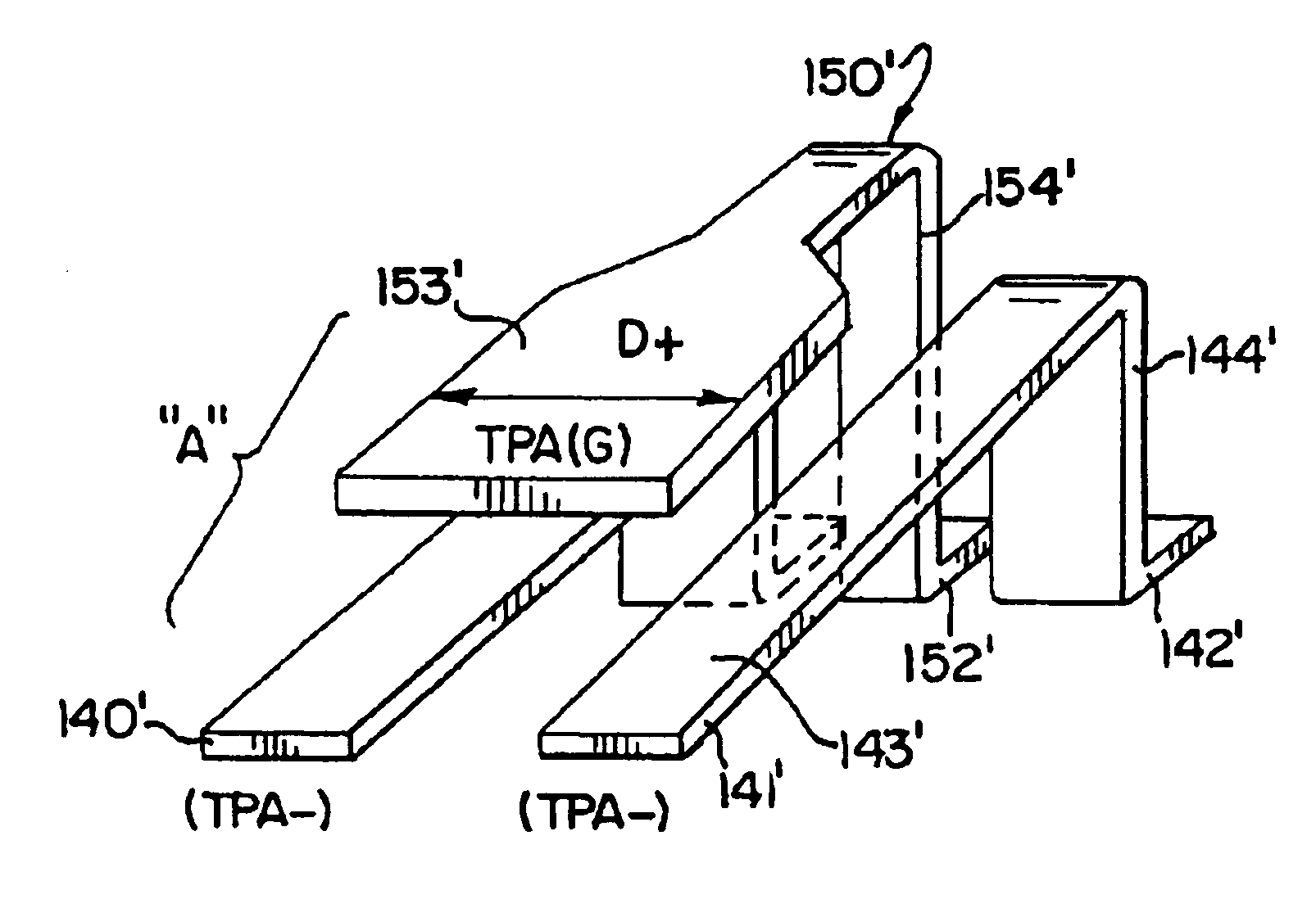
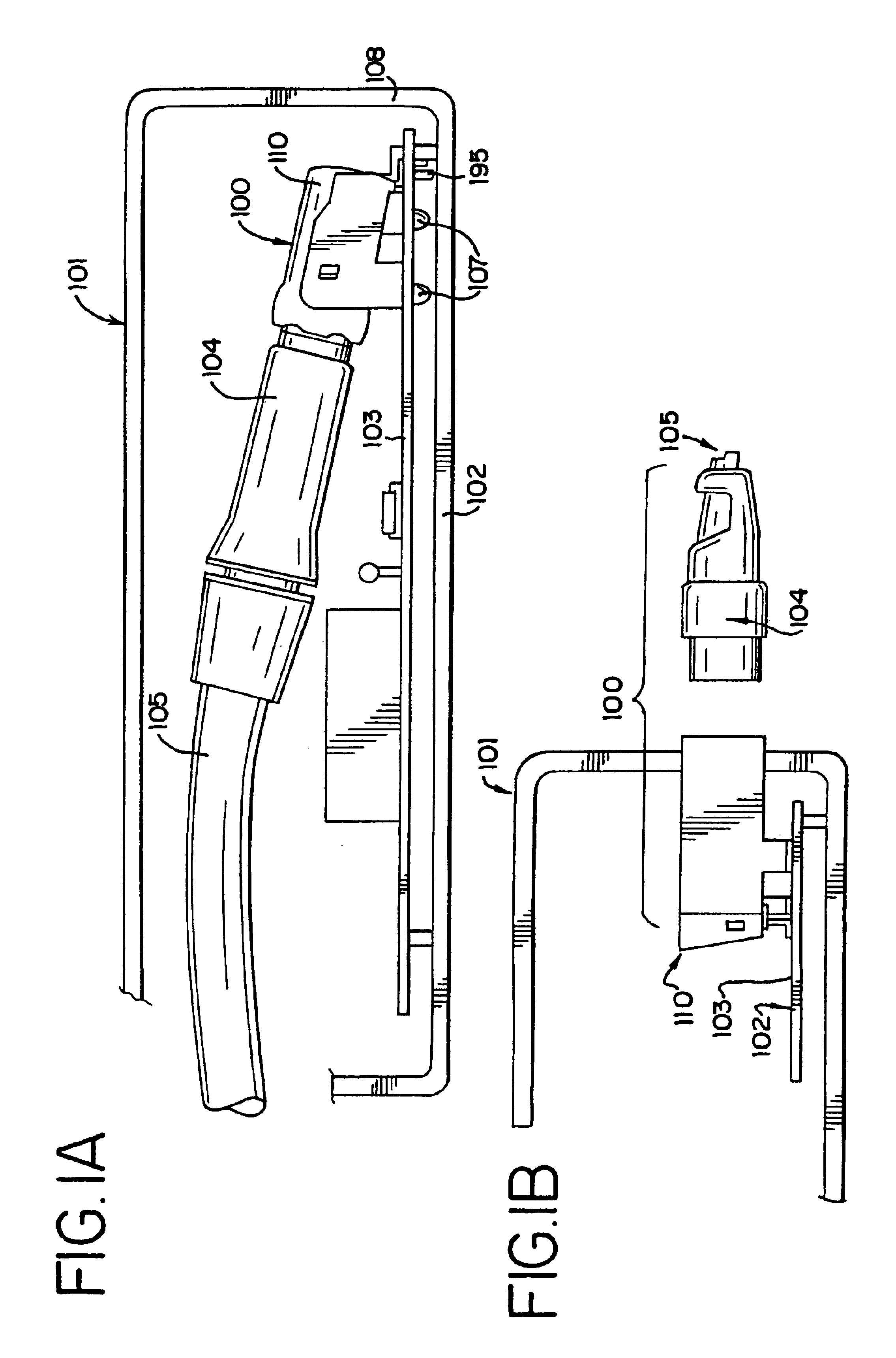
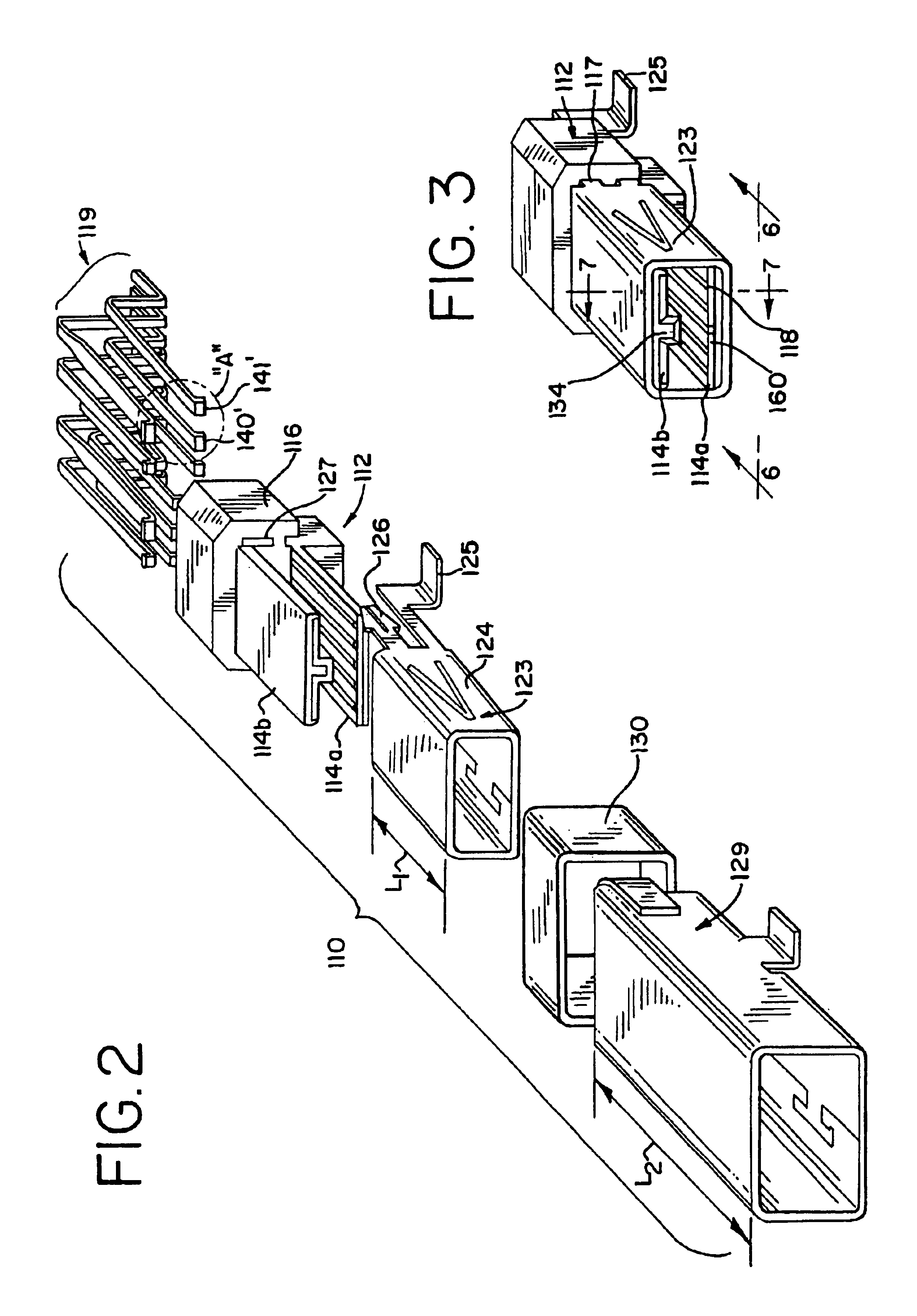
[0048]The present invention is directed to an improved connector particularly useful in enhancing the performance of high-speed cables, particularly in input-output (“I / O”) applications as well as other type of applications. More specifically, the present invention attempts to impose a measure of mechanical and electrical uniformity on the termination area of the connector to facilitate its performance, both alone and when combined with an opposing connector.

[0049]Many peripheral devices associated with an electronic device, such as a video camera or camcorder, transmit digital signals at various frequencies. Other devices associated with a computer, such as the CPU portion thereof, operate at high speeds for data transmission. High speed cables are used to connect these devices to the CPU and may also be used in some applications to connect two or more CPUs together. A particular cable may be sufficiently constructed to convey high speed signals and may include differential pairs o...


PUM


Abstract

A termination structure for mating a cable connector to a circuit board has a ground terminal and two signal terminals arranged in triangular pattern through the connector in order to reduce the impedance through the connector. The width of the ground terminal increases along its extent with respect to the signal terminals. This increase occurs along either a transition or contact portion of the ground terminal.

Description

REFERENCE TO RELATED APPLICATIONS[0001]This application is a continuation application of prior application Ser. No. 09 / 607,234, filed Jun. 30, 2000, issued as U.S. Pat. No. 6,457,983 on Oct. 1, 2002, which is a continuation-in-part of prior application Ser. No. 09 / 356,205, filed Jul. 16, 1999, now U.S. Pat. No. 6,280,209.BACKGROUND OF THE INVENTION[0002]The present invention relates generally to terminations for connectors and more particularly to connectors used in connections with signal cables, especially high-speed signal cables, and printed circuit boards.[0003]Many electronic devices rely upon transmission lines to transmit signals between related devices or between peripheral devices and circuit boards of a computer. These transmission lines incorporate signal cables that are capable of high-speed data transmissions.[0004]These signal cables may use what are known as one or more twisted pairs of wires that are twisted together along the length of the cable, with each such twi...

Claims


Application Information

Patent Timeline
Patent Type & Authority Patents(United States)
IPC IPC(8): H01R12/00H01R12/16H01R13/658H01R4/58H01R4/66H01R12/72H01R13/6471H01R13/6473H01R13/6474H01R13/652H01R13/6585H01R24/00H05K5/02
CPCH01R12/724H01R13/6471H01R13/6473H01R13/6585H01R13/6474
Inventor BASSLER, MAXWILL P.BRUNKER, DAVID L.DAWIEDCZYK, DANIEL L.LOPATA, JOHN E.
Owner MOLEX INC
Why Eureka
Try Eureka