
Mounting of semiconductor-on-diamond wafers for device processing

a technology of semiconductors and diamonds, applied in semiconductor devices, semiconductor/solid-state device details, electrical devices, etc., can solve the problems of high cost of diamond carrier substrates, time-consuming bonding process, and low thermal expansion coefficient of free standing gan-on-diamond wafers, so as to achieve a lower thermal expansion coefficient and high thermal expansion coefficien

Active Publication Date: 2020-07-16
RFHIC
View PDF0 Cites 0 Cited by
  • Summary
  • Abstract
  • Description
  • Claims
  • Application Information

AI Technical Summary

Problems solved by technology

Currently, free standing GaN-on-diamond wafers do not meet many of these specifications.
One problem with this approach is that the diamond carrier substrate is expensive and the bonding process can be time consuming.
The bonding layer is substantially unsusceptible to outgassing in ultrahigh vacuum environments and is impervious to substantial chemical and structural degradation during thermal processing at temperatures at least up to about 500° C. However, one problem with this approach is that if there is a mismatch in coefficient of thermal expansion (CTE) between the substrate and the carrier then the heating process can lead to thermally induced stress and wafer bowing.

Method used


Image

  • Mounting of semiconductor-on-diamond wafers for device processing
  • Mounting of semiconductor-on-diamond wafers for device processing
  • Mounting of semiconductor-on-diamond wafers for device processing

Examples


Embodiment Construction

[0038]One skilled in the art shall recognize: (1) that certain steps may optionally be performed; (2) that steps may not be limited to the specific order set forth herein; and (3) that certain steps may be performed in different orders, including being done contemporaneously.

[0039]Reference in the specification to “one embodiment,”“preferred embodiment,”“an embodiment,” or “embodiments” means that a particular feature, structure, characteristic, or function described in connection with the embodiment is included in at least one embodiment of the invention and may be in more than one embodiment. The appearances of the phrases “in one embodiment,”“in an embodiment,” or “in embodiments” in various places in the specification are not necessarily all referring to the same embodiment or embodiments.

[0040]The mounting of a semiconductor-on-diamond wafer to a carrier substrate in order to meet strict mechanical and geometric requirements for subsequent semiconductor device processing has be...


PUM

PropertyMeasurementUnit
temperatureaaaaaaaaaa
temperaturesaaaaaaaaaa

Abstract

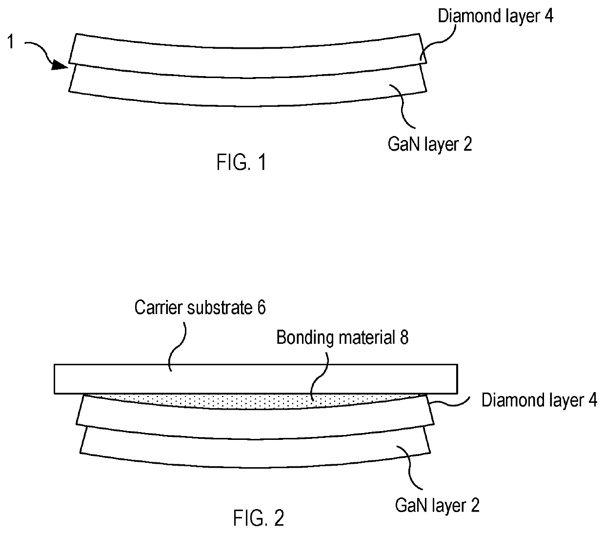
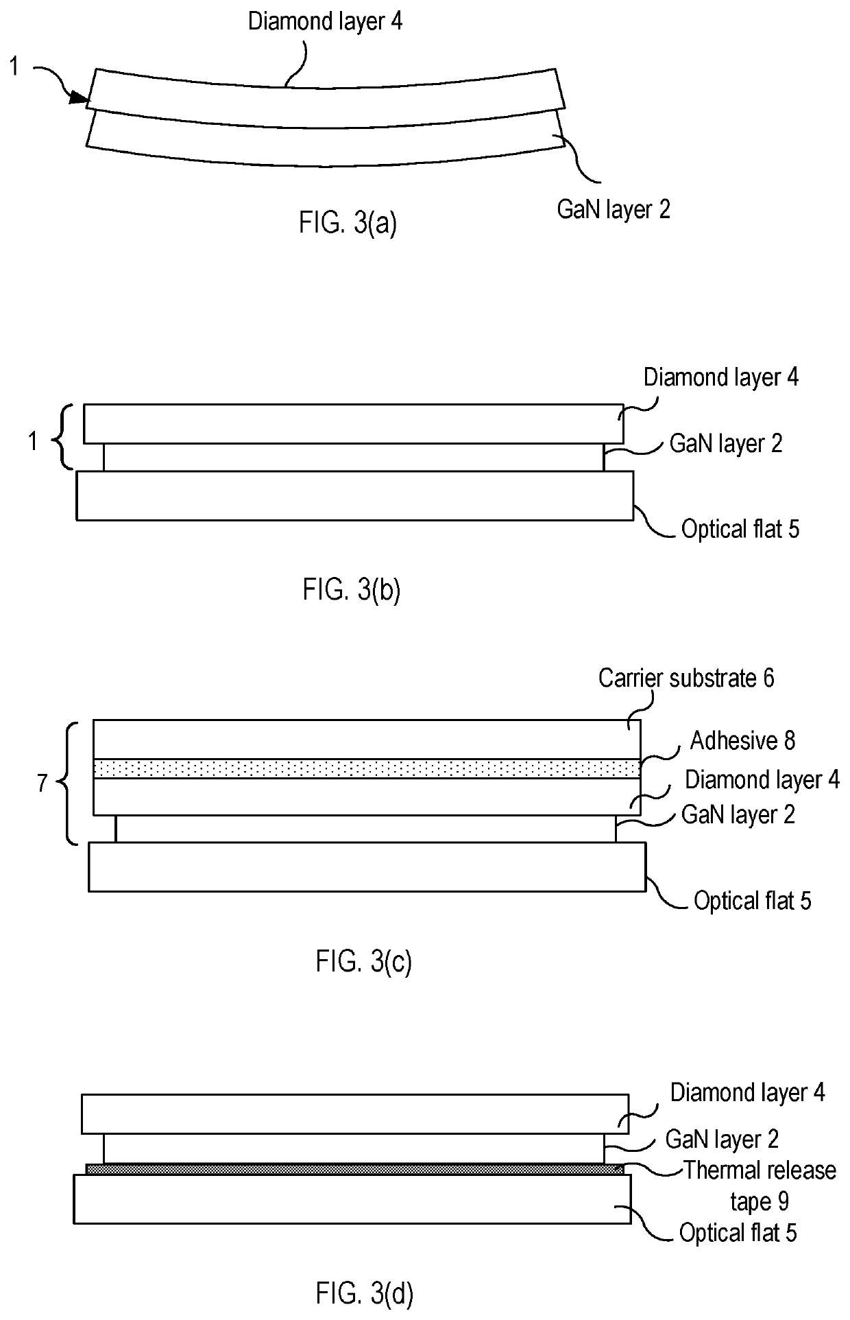
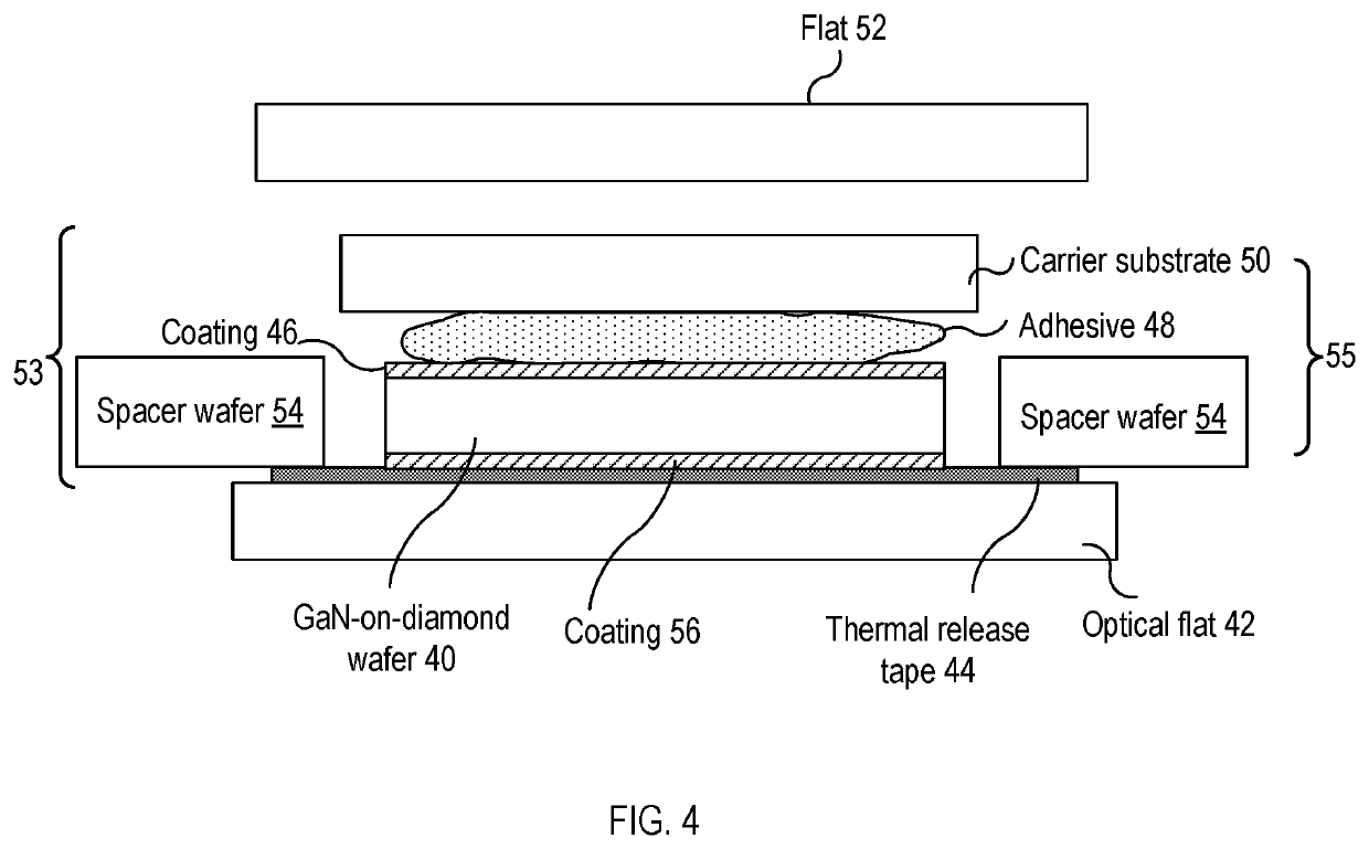
The present invention discloses a semiconductor-on-diamond-on-carrier substrate wafer. The semiconductor-on-diamond-on-carrier wafer comprises: a semiconductor-on-diamond wafer having a diamond side and semiconductor side; a carrier substrate disposed on the diamond side of the semiconductor-on-diamond wafer and including at least one layer having a lower coefficient of thermal expansion (CTE) than diamond; and an adhesive layer disposed between the diamond side of the semiconductor-on-diamond wafer and the carrier substrate to bond the carrier substrate to the semiconductor-on-diamond wafer. The semiconductor-on-diamond-on-carrier substrate wafer has the following characteristics: a total thickness variation of no more than 40 μm; a wafer bow of no more than 100 μm; and a wafer warp of no more than 40 μm.

Description

CROSS-REFERENCE TO PRIOR APPLICATIONS[0001]This application is a divisional application of U.S. patent application Ser. No. 15 / 770,209, filed on Apr. 22, 2018, which is a national Stage Patent Application of PCT International Patent Application No. PCT / US2016 / 061436, filed on Nov. 10, 2016 under 35 U.S.C. § 371, which claims priority of U.S. Patent Application No. 62 / 257,786, filed on Nov. 20, 2015, which are all hereby incorporated by reference in their entirety.FIELD OF INVENTION[0002]The present invention relates to a method of mounting a semiconductor-on-diamond wafer on a carrier substrate for subsequent semiconductor device fabrication on the semiconductor-on-diamond wafer. The present invention also relates to a semiconductor-on-diamond-on-carrier substrate wafer fabricated using the methodology described herein and to a method of fabricating one or more semiconductor device structures on a semiconductor side of such a semiconductor-on-diamond-on-carrier substrate wafer.BACKG...

Claims


Application Information

Patent Timeline
Patent Type & Authority Applications(United States)
IPC IPC(8): H01L21/683H01L21/20H01L21/02H01L29/16
CPCH01L2221/68381H01L21/02002H01L29/1602H01L21/6835H01L21/2007H01L23/3732H01L21/02269H01L21/02376H01L21/0405H01L21/324
Inventor FRANCIS, DANIELLOWE, FRANK YANTISPEARSON, MICHAEL IAN
Owner RFHIC
Learn More