Wafer separation technique for the fabrication of free-standing (Al,In,Ga)N wafers

a separation technique and free-standing technology, applied in the direction of polycrystalline material growth, crystal growth process, after-treatment details, etc., can solve the problems of under-use of free-standing gan substrates, cracking of nitride films and/or substrates, etc., to reduce the deleterious effects of stress, eliminate undesirable cracking of films and substrates, and encourage cleavage of composite systems

Inactive Publication Date: 2006-10-19
JAPAN SCI & TECH CORP
View PDF46 Cites 66 Cited by
  • Summary
  • Abstract
  • Description
  • Claims
  • Application Information

AI Technical Summary

Benefits of technology

[0020] A further object of this invention is to minimize the deleterious effects of stress induced by thermal expansion coefficient mismatch in nitride heteroepitaxy. Thermal expansion coefficient mismatch between a (Al, In, Ga)N film and its foreign substrate frequently causes cracking of the nitride film and/or the substrate upon cooling from the film growth temperature. This invention eliminates undesirable cracking of the film and substrate by encouraging cleavage o...

Problems solved by technology

However, because of the difficulties in and cost of fabricating bulk GaN crystals, free-standing GaN substrates are underused in GaN-based device applications.
Thermal expansion coe...

Method used


Image

  • Wafer separation technique for the fabrication of free-standing (Al,In,Ga)N wafers
  • Wafer separation technique for the fabrication of free-standing (Al,In,Ga)N wafers

Examples


example 1

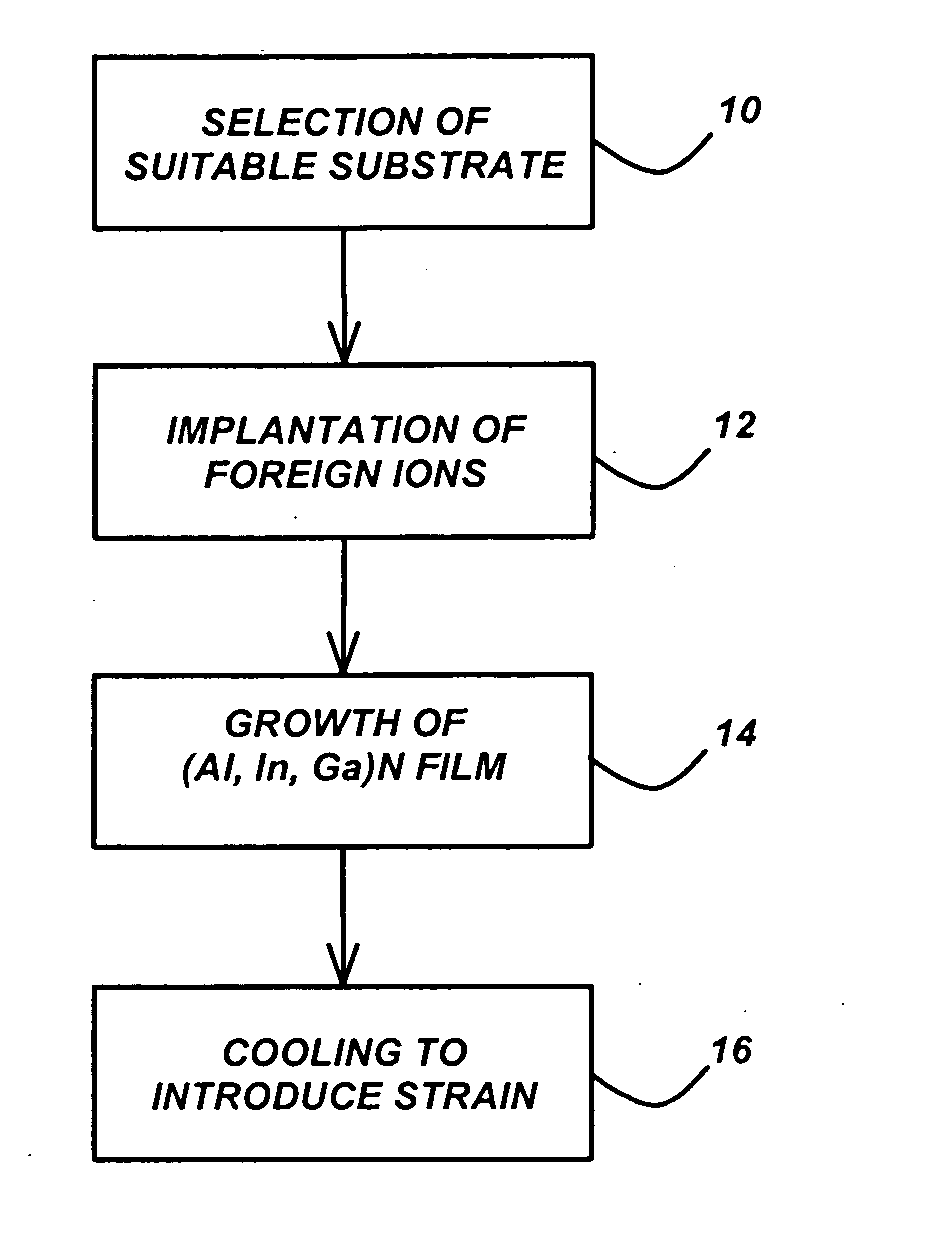
[0038] An m-plane 6H-SiC substrate is implanted with a dose of He+ ions with a peak concentration of 5×1016 cm−2 at a depth of 900 nm from the surface. The substrate is then loaded into a HVPE reactor, in which a 300 μm thick m-plane Al0.5Ga0.5N film is grown at 1200° C. During the course of the growth, the He+ ions migrate laterally and coalesce to form microvoids approximately on a plane parallel to the SiC m-plane. Upon cooling, stress due to thermal expansion mismatch causes the m-plane SiC substrate to spontaneously cleave at the microvoided layer. The remaining SiC substrate is re-polished and used for a subsequent growth. The m-plane AlGaN film now exists as a free-standing wafer with an approximately 900 nm thick SiC membrane attached to its back side. This SiC membrane is allowed to remain in place as it will not affect subsequent growth on the AlGaN growth surface.

example 2

[0039] A c-plane Al2O3 substrate is implanted with a dose of H+ ions with a peak concentration of 3×1016 cm−2 at a depth of 1000 nm from the surface. The substrate is then loaded into a HVPE reactor, in which a 300 μm thick Si-doped c-plane GaN film is grown at 1050° C. During the course of the growth, the H+ ions migrate laterally and coalesce to form microvoids approximately on a plane parallel to the Al2O3 c-plane. Upon cooling, thermal expansion mismatch related strain causes the c-plane Al2O3 substrate to spontaneously cleave at the microvoided layer. The c-plane GaN film now exists as a free-standing wafer with an approximately 1000 nm thick Al2O3 membrane attached to its back side. The Al2O3 membrane is removed by brief chemi-mechanical polishing to facilitate backside electrical contacting of subsequently grown devices on the free-standing GaN substrate.

example 3

[0040] An r-plane Al2O3 substrate is implanted with a dose of Ar+ ions with a peak concentration of 1×1017 cm−2 at a depth of 500 nm from the surface. The substrate is then loaded into a HVPE reactor, in which a 200 μm thick Si-doped a-plane GaN film is grown at 1050° C. Following the growth of this thick GaN film, a 5 μm-thick pn-junction diode structure is grown by adding Si and Mg to subsequent layers. During the course of the growth, the Ar+ ions migrate laterally and coalesce to form microvoids approximately on a plane parallel to the Al2O3 r-plane. Upon cooling, thermal expansion mismatch related strain causes the r-plane Al2O3 substrate to spontaneously cleave at the microvoided layer. The a-plane GaN film and diode now exist as a free-standing wafer with an approximately 500 nm thick Al2O3 membrane attached to the back side of the nitride film. The Al2O3 removed by brief chemi-mechanical polishing to facilitate backside contacting to the n-type region of the pn-junction diod...


PUM


Abstract

A method of fabricating free-standing (Al, In, Ga)N substrates, by in situ separation of thick epitaxially grown nitride films from their foreign substrates. A suitable substrate for (Al, In, Ga)N film growth is selected, and foreign ions are implanted in the substrate to form a comparatively sharp concentration profile. An (Al, In Ga)N film is deposited on the substrate, and the deposited film is cooled to introduce thermal expansion mismatch-related strain, so that the film spontaneously separates from the substrate.

Description

CROSS-REFERENCE TO RELATED APPLICATIONS [0001] This application claims the benefit under 35 U.S.C. Section 119(e) of the following co-pending and commonly-assigned U.S. patent application: [0002] United States Provisional Patent Application Ser. No. 60 / 670,810, filed on Apr. 13, 2005, by James S. Speck, Troy J. Baker, and Benjamin A. Haskell, entitled “WAFER SEPARATION TECHNIQUE FOR THE FABRICATION OF FREE-STANDING (Al, In, Ga)N WAFERS,” attorneys' docket no. 30794.131-US-P1; [0003] which application is incorporated by reference herein. [0004] This application is related to the following co-pending and commonly-assigned applications: [0005] U.S. Utility Patent Application Ser. No. ______, filed on same date herewith, by James S. Speck, Benjamin A. Haskell, P. Morgan Pattison and Troy J. Baker, entitled “ETCHING TECHNIQUE FOR THE FABRICATION OF THIN (Al, In, Ga)N LAYERS,” attorneys' docket no. 30794.132-US-Ul (2005-482-2), which application claims the benefit under 35 U.S.C. Section ...

Claims


Application Information

Patent Timeline
IPC IPC(8): H01L21/3205H01L21/28H01L21/44H01L21/4763
CPCC30B25/02C30B25/18C30B29/403C30B33/00H01L21/0237H01L21/02378H01L21/76254H01L21/02433H01L21/02472H01L21/0254H01L21/02658H01L21/265H01L21/26506H01L21/0242
Inventor SPECK, JAMES S.BAKER, TROY J.HASKELL, BENJAMIN A.
Owner JAPAN SCI & TECH CORP
Why Eureka
Try Eureka