Structure for packaging and method for manufacturing the same

Inactive Publication Date: 2020-07-30
TYNTEK
View PDF0 Cites 0 Cited by
  • Summary
  • Abstract
  • Description
  • Claims
  • Application Information

AI Technical Summary

Benefits of technology

The patent text describes a structure for packaging and a method of manufacturing it. The structure includes a gap between the metal and insulation layers to prevent metal spills. The technical effect of this is to improve the reliability and stability of the packaging structure.

Problems solved by technology

Unfortunately, the tin-ball bonding method cannot meet the requirements of light weight, compact size, and high density.
Nonetheless, this connecting method induces another problem.
During the pressing and bonding processes, the softened close-to-the-liquid-phase bonding pads may spill some metal blocks or strips, leading to leakage current or short circuit.

Method used


Image

  • Structure for packaging and method for manufacturing the same
  • Structure for packaging and method for manufacturing the same
  • Structure for packaging and method for manufacturing the same

Examples


second embodiment

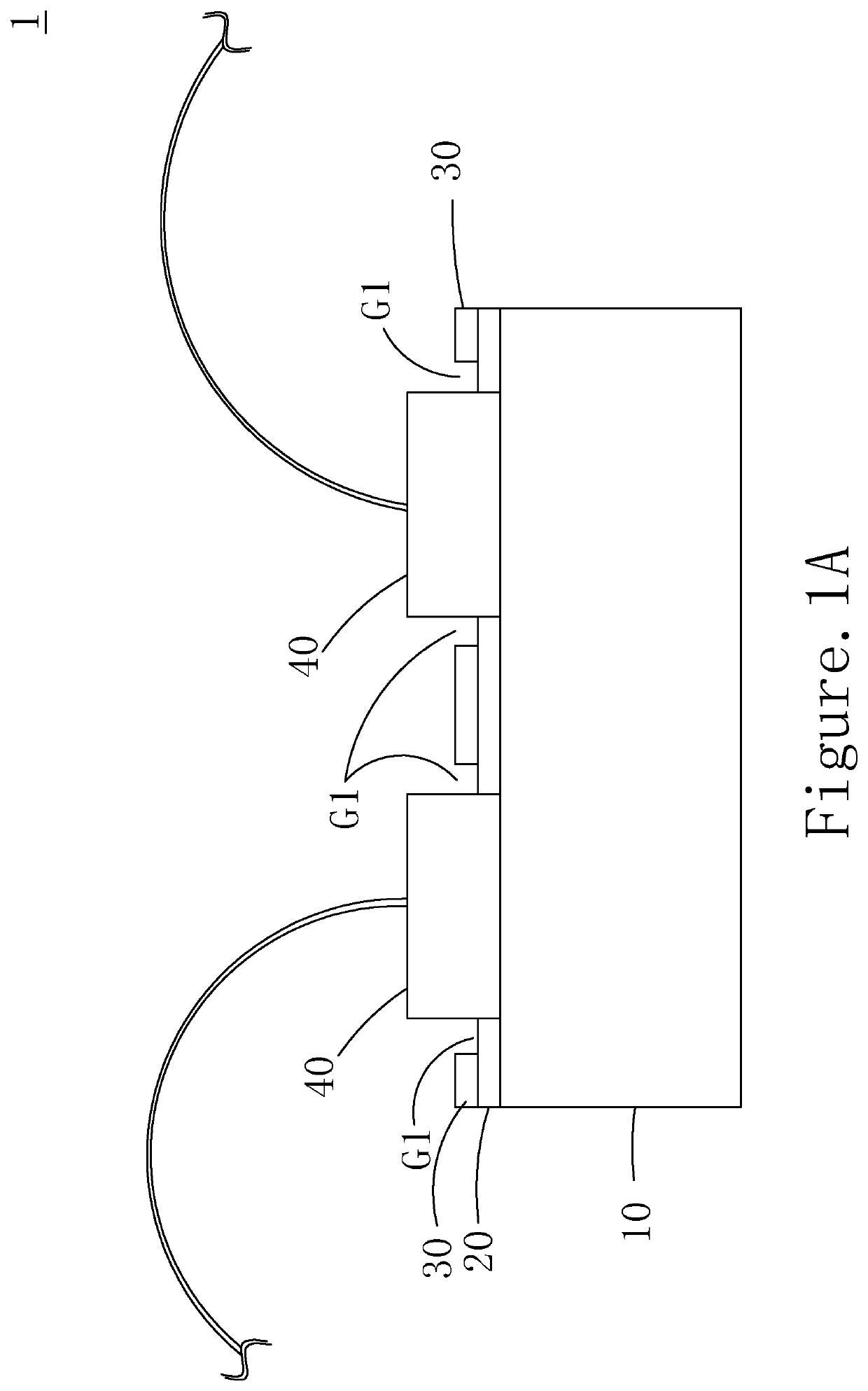
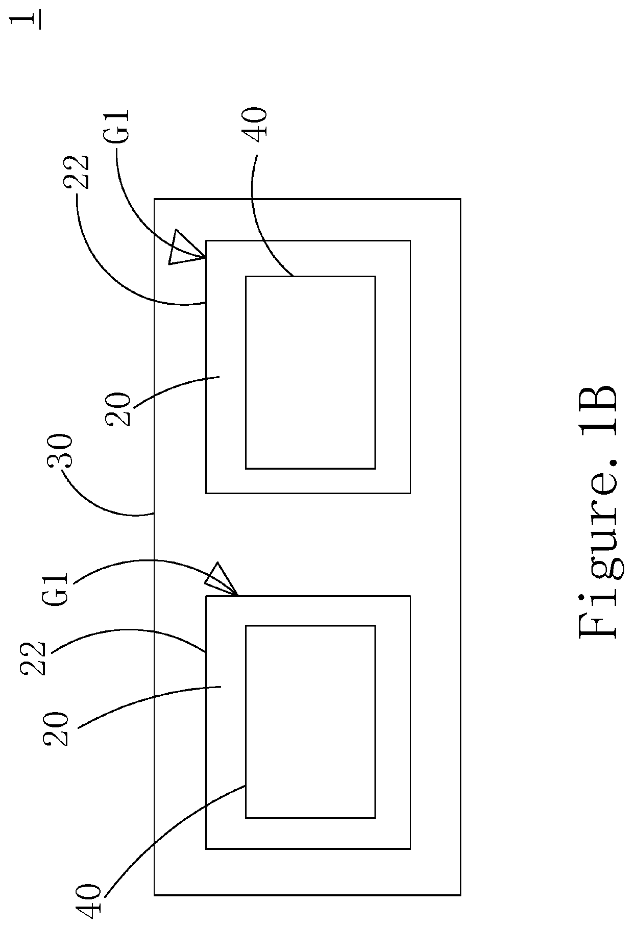
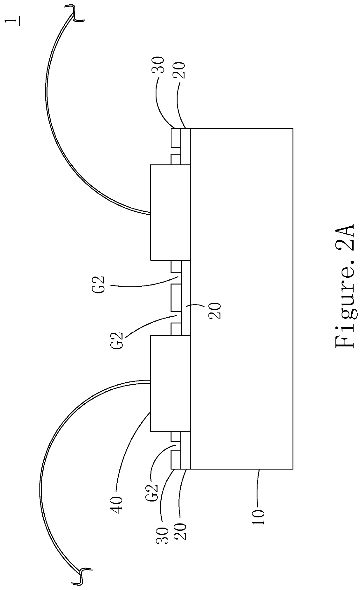
[0050]As shown in FIG. 2A, the difference between the second embodiment and the first one shown in FIG. 1A is that in FIG. 1A, the first gap G1 is located between the first insulation layer 30 and one of the two or more metal members 40. In FIG. 2A, the insulation layer 30 is attached to the two or more metal members 40, and a second gap G2 is disposed on the oxide layer 20. As shown in FIG. 2B, the second gap G2 is disposed annularly on the oxide layer 20. There is a spacing distance D between the second gap G2 and the two or more metal members 40. The second gap G2, like an annular trench, is disposed surrounding the two or more metal members 40 with the function identical to that of the first gap G1. Hence, the details will not be described again.

third embodiment

[0051]As shown in FIG. 3A, the difference between the third embodiment and the first one shown in FIG. 1A is that in FIG. 1A, the first gap G1 is located on the oxide layer 20. In FIG. 3A, a third gap G3 is disposed below the first gap G1. The third gap G3 is disposed between the oxide layer 20 and one of the two or more metal members 40. The oxide layer 20 and the first insulation layer 30 include gaps corresponding to the two or more metal members 40. Namely, the third gap G3 is equivalent to the first gap G1 extending vertically to the semiconductor device 10. As shown in FIG. 3B, the oxide layer 20 includes an accommodation space 24 with a larger area, forming the third gap G3 surrounding the two or more metal members 40. The surface of the semiconductor device 10 can be seen through the third gap G3. In addition, the function of the third gap G3 is identical to that of the first gap G1. Hence, the details will not be described again.

[0052]Please refer to FIG. 4A, which shows a ...


PUM


Abstract

The present invention relates to a structure for packaging and the method for manufacturing the same. The structure for packaging comprise two or more metal members disposed on a substrate or a semiconductor device. A patterned layer and an insulation layer are disposed surrounding the metal members. There is a gap between the patterned layer and the insulation layer. Thereby, while bonding the metal members, metal spilling can be avoided, for further preventing the structure from short circuit or current leakage.

Description

FIELD OF THE INVENTION[0001]The present invention related to a semiconductor structure and the method for manufacturing the same, and particularly to a structure for packaging and the method for manufacturing the same.BACKGROUND OF THE INVENTION[0002]In the semiconductor packaging industry, tin-ball bonding is extensively adopted for forming electrical connection between an integrated-circuit die and a die carrier such as a lead frame or a substrate. In a tin-ball bonding process according to the prior art, the energy selected from the group consisting of heat, pressure and ultrasound is adopted to form a metal connection or soldering between a connecting wire and a connecting pad. As portable electronic products develop prosperously in recent years, various products are developed toward the trend of high density, high performance, light weight, and compact size; various types of package on package are developed as well. Unfortunately, the tin-ball bonding method cannot meet the req...

Claims


Application Information

Patent Timeline
IPC IPC(8): H01L23/498H01L21/02
CPCH01L21/02403H01L21/02282H01L23/49822H01L23/49894H01L21/02488H01L23/49838H01L21/4846H01L23/12H01L23/3171H01L23/3192H01L24/14H01L24/05H01L2224/03334H01L2224/05567H01L2224/05572H01L2224/10175H01L2224/05553H01L24/03H01L24/81H01L2224/81815H01L2224/0401H01L2224/04042H01L2224/48491H01L2224/48996H01L24/48H01L2224/11334H01L2224/13022H01L2224/13021H01L24/11H01L24/13H01L2224/10145H01L2224/81191H01L2224/81192H01L2224/85815H01L24/85H01L2224/13013H01L2224/05557H01L2224/16227H01L2224/1403H01L2224/06102H01L2924/19107H01L24/16H01L24/17H01L2224/17104H01L2924/3841H01L2924/00012H01L24/10H01L2224/10135
Inventor CHOU, CHIN-HANCHANG, WEI-YULIN, GUAN-CHENLIN, I-HSIEN
Owner TYNTEK
Why Eureka
Try Eureka