

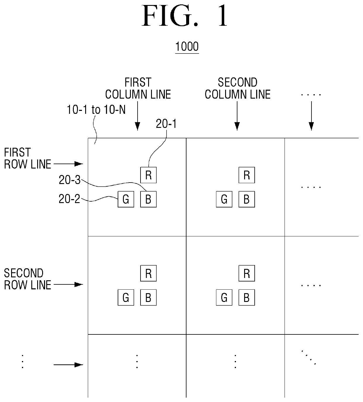
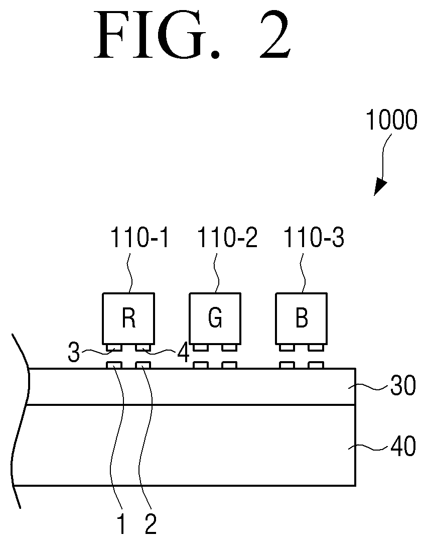
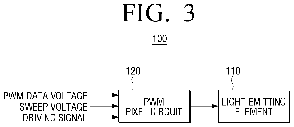
Display panel and driving method of the display panel
a technology of display panel and driving method, which is applied in the direction of instruments, static indicating devices, etc., can solve the problems of low decreased light emission duty ratio, and inadequacies of low power consumption
- Summary
- Abstract
- Description
- Claims
- Application Information
AI Technical Summary
Benefits of technology
Problems solved by technology
Method used
Image

Examples
Embodiment Construction
[0060]According to embodiments, a display panel wherein a data voltage can be stably set and a high light emission duty ratio can be secured, and a driving method of the display panel can be provided. Accordingly, low power consumption in various types of display panels such as an inorganic LED display panel becomes possible.
[0061]In explaining the disclosure, in case it is determined that detailed explanation of related known technologies may unnecessarily confuse the gist of the disclosure, the detailed explanation will be omitted. Also, overlapping explanation about the same components will be omitted as much as possible.
[0062]The suffix “part” for components used in the following description is provided or interchangeably used in consideration of only easiness of drafting the specification, and does not have meaning or a function of itself distinguishing it from other components.
[0063]The terms used in the disclosure are used to explain the embodiments, and are not intended to r...
PUM
| Property | Measurement | Unit |
|---|---|---|
| size | aaaaa | aaaaa |
| sweep voltage | aaaaa | aaaaa |
| time period | aaaaa | aaaaa |
Abstract
Description
Claims
Application Information