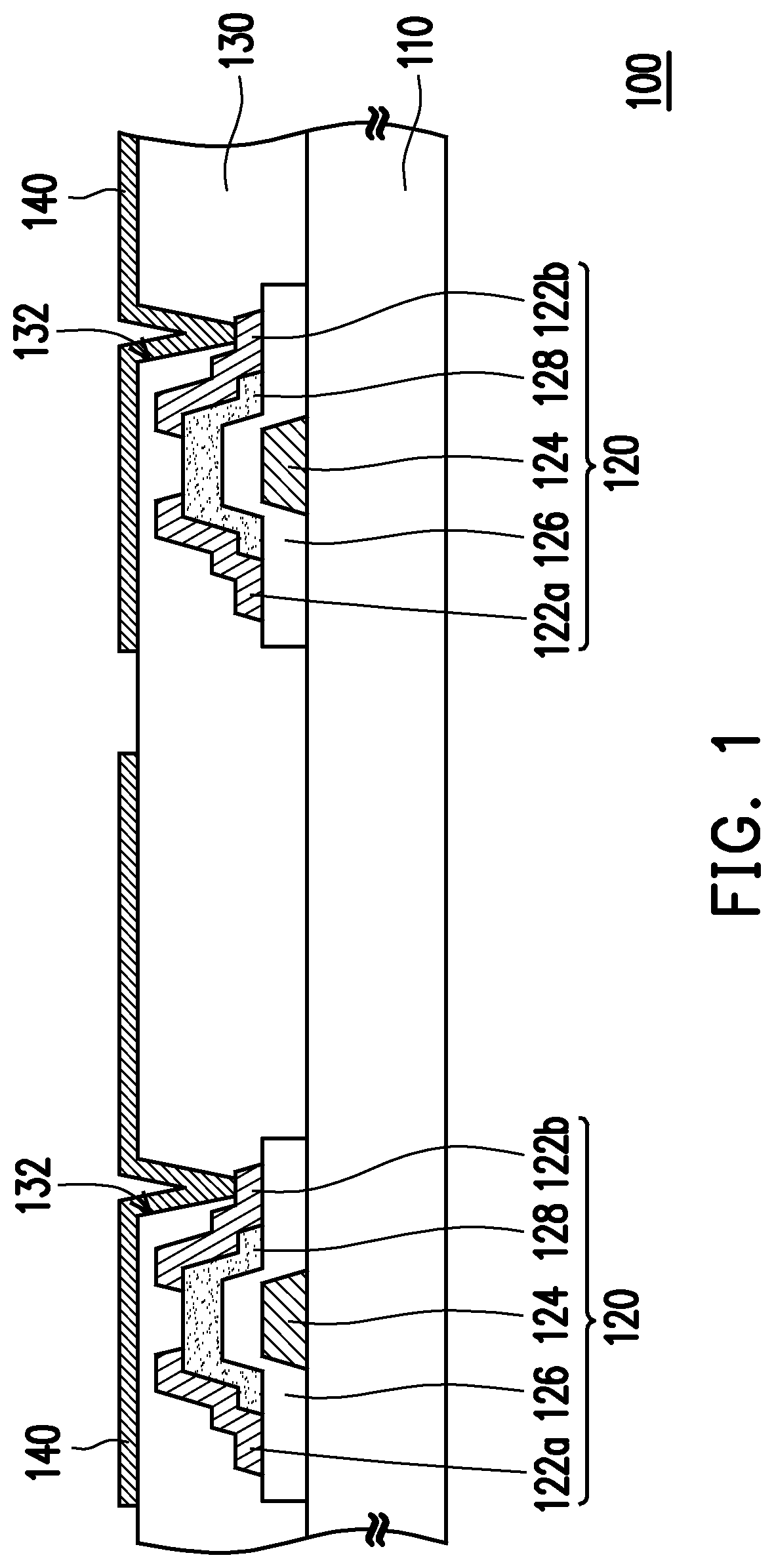
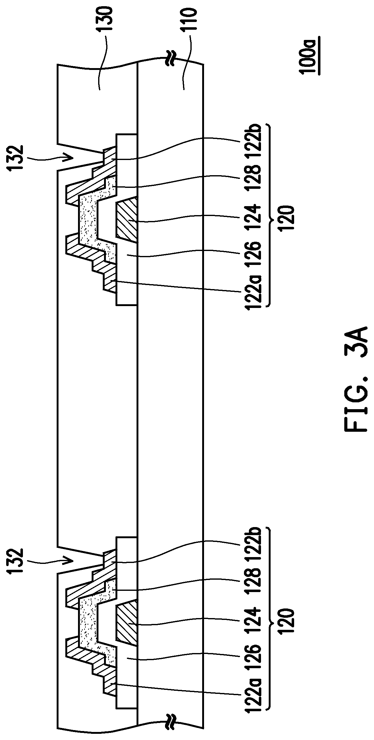
[0027]FIG. 1 is a cross-sectional schematic view of a reflective active device array substrate of an embodiment of the disclosure. Please refer to FIG. 1, a reflective active device array substrate 100 of the present embodiment includes a substrate 110, a plurality of active devices 120 (Only two are drawn schematically in FIG. 1), a protective layer 130 and a plurality of metal oxide conductor layers 140 (only two are drawn schematically in FIG. 1). The active devices 120 are dispersedly disposed on the substrate 110. The protective layer 130 is disposed on the substrate 110 and covers the active devices 120. The protective layer 130 has a plurality of openings 132 (only two are drawn schematically in FIG. 1), and each of the openings 132 respectively exposes a source 122a or a drain 122b of the corresponding active devices 120. The metal oxide conductor layers 140 are disposed on the substrate 110 and cover the protective layer 130. Each of the metal oxide conductor layers 140 is electrically connected to the source 122a or the drain 122b of each of the corresponding active devices 120 through each of the corresponding openings 132.
[0028]Specifically, the active devices 120 of the present embodiment include a gate 124, a semiconductor channel layer 128, a gate insulating layer 126, the source 122a and the drain 122b. The gate 124 is located on the substrate 110, and the gate insulating layer 126 covers the gate 124 and a portion of the substrate 110. The semiconductor channel layer 128 is located on a side of the gate insulating layer 126 opposite to the gate 124 and does not contact the gate 124, which means that the gate insulating layer 126 is disposed between the gate 124 and the semiconductor channel layer 128. The source 122a and the drain 122b are disposed on a same side of the semiconductor channel layer 128, and expose a portion of the semiconductor channel layer 128. Herein, from a way of arranging the gate 124, the gate insulating layer 126, the semiconductor layer 128, the source 122a and the drain 122b, it can be known that the active devices 120 of the present embodiment are specifically made as a bottom gate thin film transistor, but is not limited hereto. The disclosure does not limit a structure type of the active devices 120. In other embodiments, the active devices may also be a top gate thin film transistor, which still belongs to the scope desired to be protected by the disclosure.
[0029]Please refer to FIG. 1, the openings 132 of the protective layer 130 of the present embodiment expose the drain 122b of the corresponding active devices 120. However, in other embodiments that are not drawn, the openings of the protective layer may also expose the source of the corresponding active devices. The metal oxide conductor layers 140 are electrically connected to the drain 122b of each of the corresponding active devices 120 through the corresponding openings 132. Herein, the metal oxide conductor layers 140 have opaqueness (which is light shielding effect), conductivity and low reflection characteristic, wherein a material of the metal oxide conductor layers 140 may be molybdenum oxide, molybdenum-niobium oxide, tantalum oxide, aluminum oxide or other metal oxides with low reflectivity.
[0030]Briefly, in the structure of the reflective active device array substrate 100 of the present embodiment, the metal oxide conductor layers 140 are used as the conductive electrode. Compared with the conventional use of a metal material as the conductive electrode, the metal oxide conductor layers 140 of the present embodiment has a lower reflectivity and can reduce external light reflection. Moreover, the metal oxide conductor layers 140 of the present embodiment do not affect the product feature of the reflective active device array substrate 100 since the material feature thereof still has opaqueness (which is light shielding effect), conductivity and reflection characteristic. In addition, the metal oxide conductor layers 140 of the present embodiment has a better anti-corrosion capability than the conductive electrode of the metal material, and the reflective active device array substrate 100 has a better product reliability.
[0031]Descriptions above only explain the structure of the reflective active device array substrate 100 of the present embodiment. Following descriptions would explain a manufacturing method of the reflective active device array substrate 100 of the present embodiment with a flow chart of FIG. 2 and cross-sectional schematic views of FIG. 3A and FIG. 3B.
[0032]FIG. 2 is a flow chart of a manufacturing method of a reflective active device array substrate of an embodiment of the disclosure. FIG. 3A to FIG. 3B are cross-sectional schematic views of the manufacturing method of the reflective active device array substrate of FIG. 2. Please refer to FIG. 2 and FIG. 3A simultaneously. Firstly, in a step S10, an array substrate 100a is provided, wherein the array substrate 100a includes the substrate 110, the plurality of active devices 120 (only two are drawn schematically in FIG. 3A) and the protective layer 130. The active devices 120 are dispersedly formed on the substrate 110, and the protective layer 130 is formed on the substrate 110 and covers the active devices 120. The protective layer 130 has the plurality of openings 132 (only two are drawn schematically in FIG. 3A), and each of the openings 132 respectively exposes the drain 122b of each of the corresponding active devices 120.
[0033]Further, please refer to FIG. 2 and FIG. 3A simultaneously. In a step S20, the array substrate 100a is moved into a reaction chamber (not drawn), wherein a metal target material (not drawn) is disposed in the reaction chamber. Herein, the target material is, for example, molybdenum, molybdenum-niobium, tantalum, or aluminum.
[0034]Afterward, please refer to FIG. 2 and FIG. 3B simultaneously. In a step S30, when a plasma (not drawn) bombards the metal target material, a reactant gas (not drawn) is pumped into the reaction chamber (not drawn) to perform a chemical reaction with the metal target material, and to form a plurality of metal oxide conductor layers 140 on the array substrate 100a. At the moment, the metal oxide conductor layers 140 cover the protective layer 130, and each of the metal oxide conductor layers 140 is electrically connected to the drain 122b of each of the corresponding active devices 120 through each of the corresponding openings 132. Herein, the reactant gas is, for example, oxygen. Thus, the manufacture of the reflective active device array substrate 100 is completed.
[0035]For example, according to the manufacturing method, if molybdenum is selected as a metal target material, molybdenum oxide may be formed through bumping into oxygen when a plasma bombards the metal target material. Compared with general metal molybdenum, about 60% of incident light can be reflected, and the molybdenum oxide with the same thickness can reflect about 6% of incident light, which significantly reduces the light reflectivity.
[0036]In brief, in the manufacturing method of the reflective active device array substrate 100 of the present embodiment, the metal oxide conductor layers 140 replace the conductive electrode of the conventional metal material. Therefore, the reflective active device array substrate 100 has low light reflectivity in addition to conductivity and light shielding effect, and can reduce external light reflection.
[0037]FIG. 4 is a cross-sectional schematic view of a reflective display apparatus of another embodiment of the disclosure. Please refer to FIG. 4. A reflective display apparatus 10 of the present embodiment includes the above reflective active device array substrate 100, and an electrophoretic display film 200, wherein the electrophoretic display film 200 is disposed on the reflective active device array substrate 100. The electrophoretic display film 200 includes a flexible substrate 210, a transparent conductive layer 220 and a display medium layer 230. The transparent conductive layer 220 is disposed on the flexible substrate 210, and is located between the reflective active device array substrate 100 and the flexible substrate 210. Herein, a material of the flexible substrate 210 may be polyethylene terephthalate (PET) or polyethylene napthalate (PEN), but is not limited hereto. A material of the transparent conductive layer 220 may be indium tin oxide (ITO), but is not limited hereto. The display medium layer 230 is disposed on the flexible substrate 210, and is located between the reflective active device array substrate 100 and the transparent conductive layer 220. The display medium layer 230 includes a plurality of display mediums 232 (only two are drawn schematically in FIG. 3), each display medium 232 includes an electrophoretic liquid 234 and a plurality of charged particles 236 distributed in the electrophoretic liquid 234. Specifically, the charged particles 236 includes a plurality of white charged particles and a plurality of black charged particles, and a movement of the black charged particles and the white charged particles may be driven by a method of adding DC voltage or AC voltage, so as to display black, white or gray of different gradations. Surely, in other embodiments that are not drawn, each of the display mediums may also include the electrophoretic liquid and the plurality of white charged particles distributed in the electrophoretic liquid, wherein the electrophoretic liquid may be, for example, a black electrophoretic liquid; or, the electrophoretic liquid and the charged particles may have other colors and are not limited hereto.
[0038]In the manufacturing process of the reflective display apparatus 10, after the reflective active device array substrate 100 is formed through the method of FIG. 2 and FIG. 3A to FIG. 3B, the electrophoretic display film 200 is assembled on the reflective active device array substrate 100 as shown in FIG. 4. Herein, the manufacture of the reflective display apparatus 10 is completed.
[0039]In brief, the reflective display apparatus 10 of the present embodiment includes the above reflective active device array substrate 100, wherein the reflective active device array substrate 100 uses the metal oxide conductor layers 140 as the conductive electrode. Compared with the conventional use of the metal material as the conductive electrode, the metal oxide conductor layers 140 of the present embodiment may reduce the reflection of external light without generating bright spots when a broken hole occurs to the electrophoretic display film 200, so as to make the reflective display apparatus 10 have a better display quality.
[0040]Based on the above, in the structure of the reflective active device array substrate of the disclosure, the metal oxide conductor layers are used as the conductive electrode. Compared with the conventional use of the metal material as the conductive electrode, the metal oxide conductor layers of the disclosure has a lower light reflectivity, and may reduce external light reflection. Therefore, the reflective display apparatus adopting the reflective active device array substrate of the disclosure may make the reflective display apparatus have a better display quality since the metal oxide conductor layer may reduce the reflection of external light without generating bright spots when a broken hole occurs to the electrophoretic display film thereof.
[0041]It will be apparent to those skilled in the art that various modifications and variations can be made to the disclosed embodiments without departing from the scope or spirit of the disclosure. In view of the foregoing, it is intended that the disclosure covers modifications and variations provided that they fall within the scope of the following claims and their equivalents.