Image display element
a technology of image display element and light emitting element, which is applied in the direction of electrical devices, semiconductor devices, instruments, etc., can solve the problems of reducing the light emission efficiency, reducing the light emission ratio of the outside of the light generated by affecting so as to improve the light emission efficiency of the micro light emitting element and prevent optical crosstalk between adjacent micro light emitting elements.
- Summary
- Abstract
- Description
- Claims
- Application Information
AI Technical Summary
Benefits of technology
Problems solved by technology
Method used
Image
Examples
embodiment 1
[0055](Configuration of Image Display Element 200)
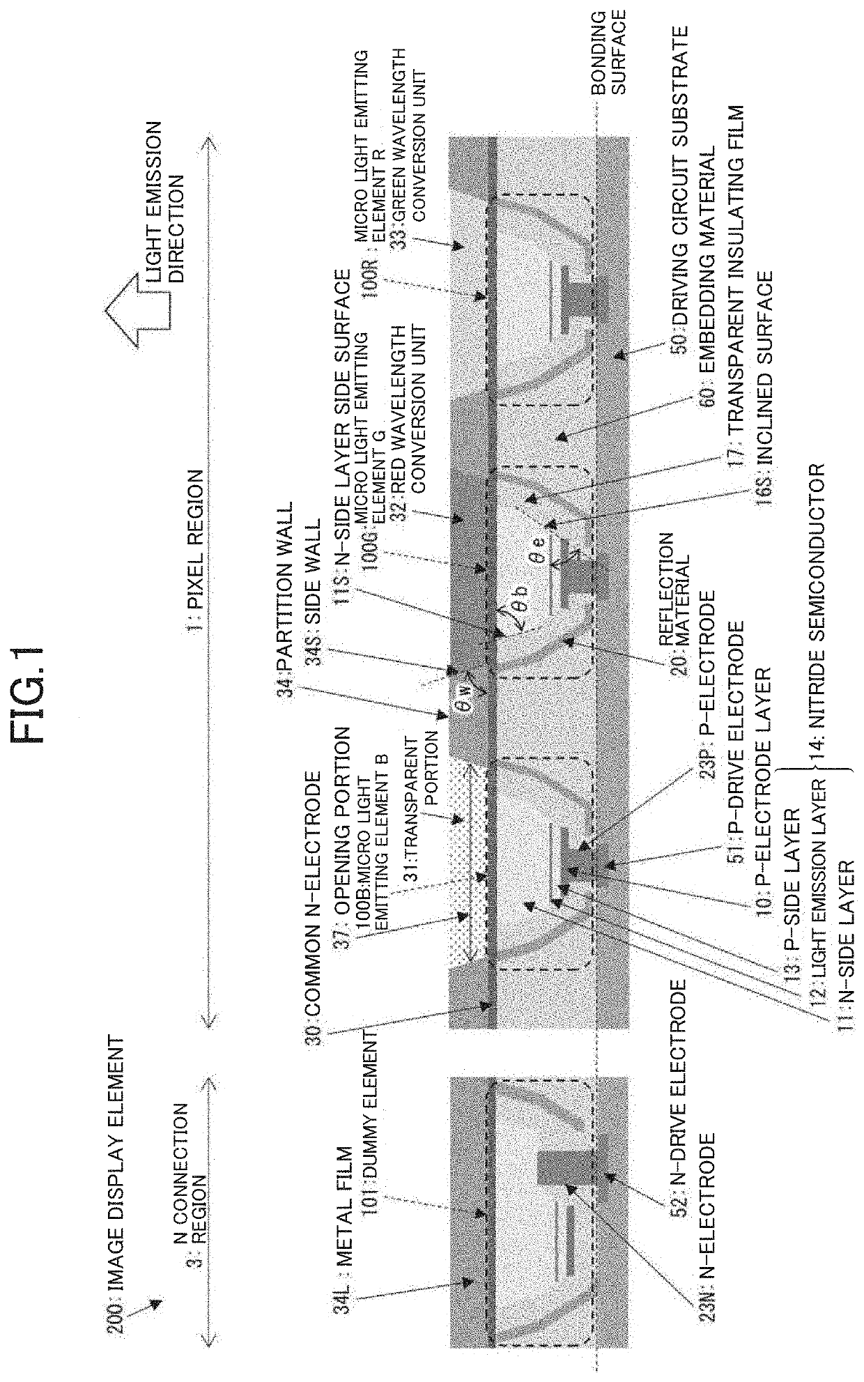
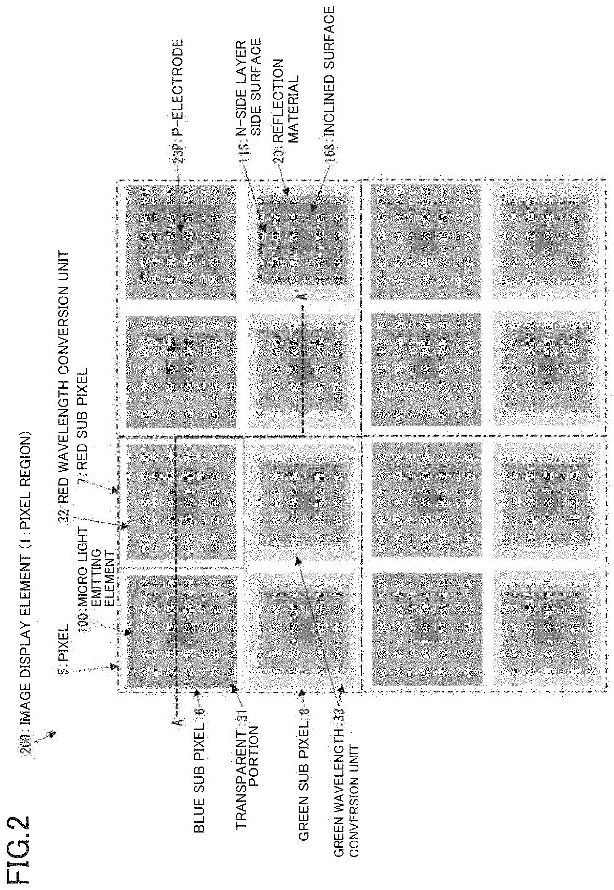
[0056]An embodiment of the present invention will be described using an image display element 200 as a display element including a plurality of micro light emitting elements 100 as an example. FIG. 1 is a schematic cross-sectional view of the image display element 200 according to Embodiment 1 of the present invention. FIG. 2 is a schematic plan view of the micro light emitting element 100 according to Embodiment 1 of the present invention. In the description of a configuration of the image display element 200, a light emitting surface is called an upper surface, a surface opposite to the light emitting surface is called a lower surface, and a side surface other than the upper surface and the lower surface is called a side surface.
[0057]As illustrated in FIG. 2, the upper surface of the image display element 200 is a pixel region 1 in which a plurality of pixels 5 are arranged in an array. Each pixel 5 includes a blue sub pixel 6 tha...
embodiment 2
[0190](Configuration of Image Display Element 200b)
[0191]Another embodiment of the present invention will be described below with reference to FIG. 10 and FIGS. 11A-11E. For convenience of description, members having the same functions as the members described in the above embodiment are denoted by the same reference numerals, and description thereof will not be repeated. The same applies to Embodiment 3 and subsequent embodiments.
[0192]In an image display element 200b of Embodiment 2, the configuration of a partition wall 34b is different from that of the image display element 200 of Embodiment 1. In the present embodiment, it is intended to realize an image display element having a finer micro light emitting element than in Embodiment 1.
[0193]As illustrated in FIG. 10, the partition wall 34b of the present embodiment has a configuration including a partition wall base material 35 and a partition wall reflection material 36. The front surface of the partition wall reflection materi...
embodiment 3
[0201](Configuration of Image Display Element 200c)
[0202]Another embodiment of the present invention will be described below with reference to FIG. 12 and FIGS. 13A-13G. An image display element 200c of Embodiment 3 has a configuration similar to that of the image display element 200b of Embodiment 2. The image display element 200c is different from the image display element 200b in that the image display element 200c is manufactured by forming the transparent portion 31 and the wavelength conversion units 32 and 33 on a substrate different from the driving circuit substrate 50 to bond to the driving circuit substrate 50 having the micro light emitting element 100.
[0203]As illustrated in the cross-sectional view of FIG. 12, the image display element 200c includes a transparent substrate 45, a light absorbing material 38, and a bandpass filter 39 on the front surface. The image display element 200c is manufactured by forming these structures, the transparent portion 31, the wavelengt...
PUM
 Abstract
Description
Claims
Application Information


