
Rear-Illuminated -Type Photodiode Array

a photodiode array and rear illumination technology, applied in the field of rear illumination type photodiode array, can solve the problems of electrical crosstalk, difficult to reduce the pitch to such a small value, and not all of the incoming lightwave is absorbed in the absorption layer, so as to prevent optical crosstalk

Inactive Publication Date: 2007-05-03
SUMITOMO ELECTRIC IND LTD
View PDF6 Cites 6 Cited by
  • Summary
  • Abstract
  • Description
  • Claims
  • Application Information

AI Technical Summary

Benefits of technology

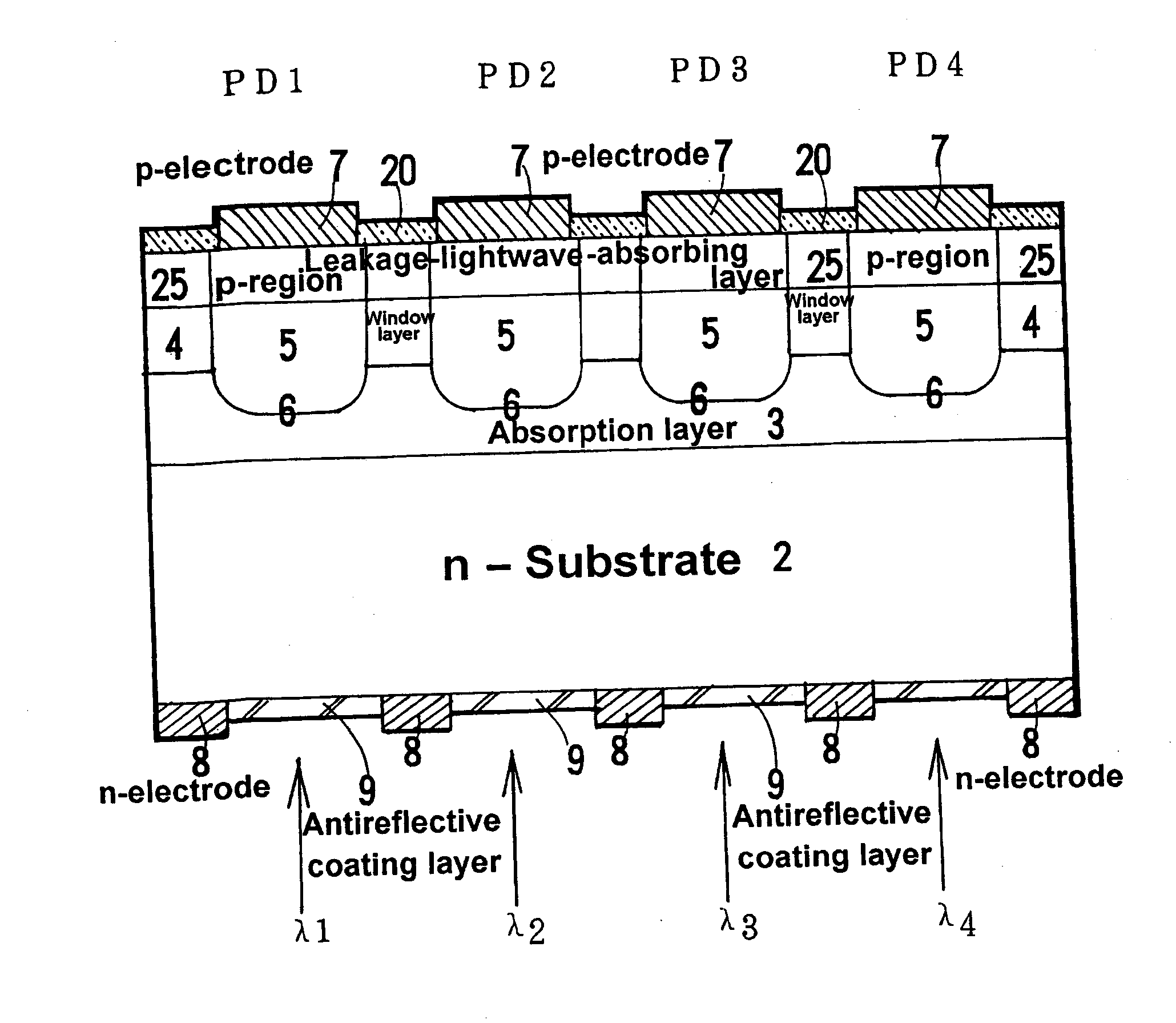
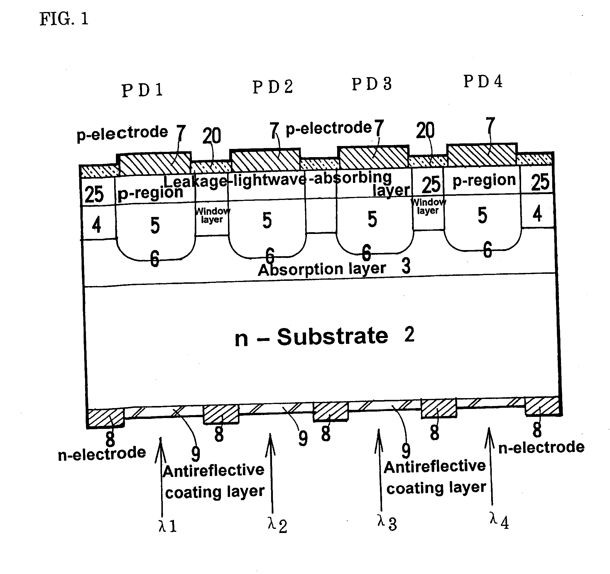
The present invention provides a rear-illuminated-type photodiode array with reduced optical crosstalk between neighboring photodiodes, which results in a higher sensitivity and less noise. This is achieved by using an antireflective coating, a leakage-lightwave-absorbing layer, and second-electroconductive-type regions that penetrate through the leakage-lightwave-absorbing layer from the top surface. The reduced optical crosstalk allows for a smaller size of the photodiode array and increased spatial resolution in a sensor.

Problems solved by technology

However, in the case of independent photodiodes, it is difficult to reduce the pitch to such a small value.
Because photodiode units having a comparable function are arranged with a small pitch, electrical crosstalk poses a problem.
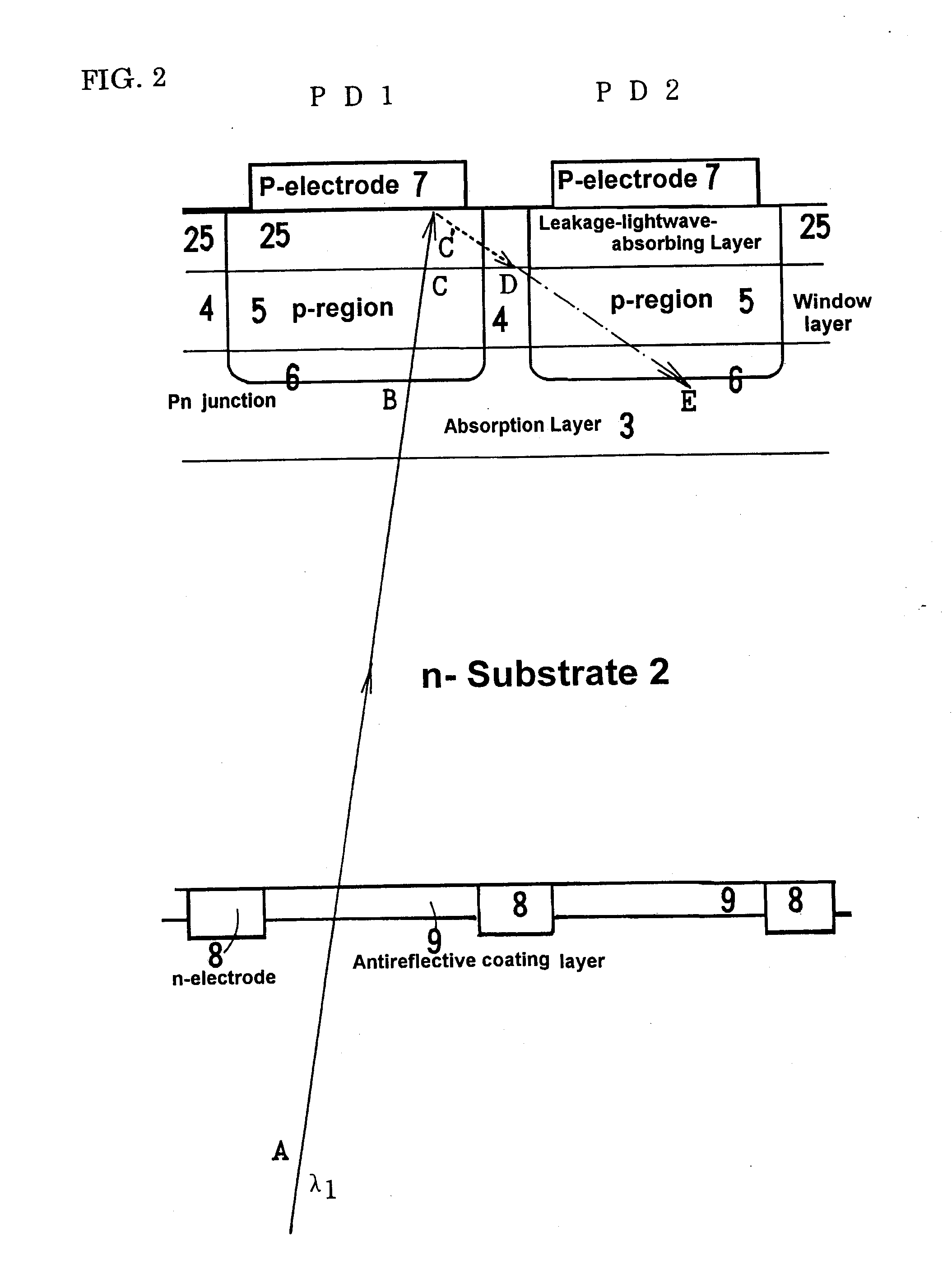
However, not all of an incoming lightwave is absorbed in the absorption layer.
In other words, a lightwave having entered a photodiode unit causes a noise to a neighboring photodiode unit.

Method used


Image

  • Rear-Illuminated -Type Photodiode Array
  • Rear-Illuminated -Type Photodiode Array
  • Rear-Illuminated -Type Photodiode Array

Examples


example 1

One-Dimensionally Arranged Photodiode Array (M×1: FIG. 3)

[0060] The method of producing a rear-illuminated-type photodiode array of the present invention shown in FIG. 3 is explained below. The following layers were epitaxially grown by the metalorganic vapor phase epitaxial method (MOVPE method) in the following order on an n-type InP substrate 2 that had a thickness of 350 μm, that was doped with sulfur, and that had a carrier concentration of n=3×1018 cm−3: [0061] an n-type InP buffer layer 30 (thickness: 2 μm, undoped, and carrier concentration: n=1×1015 cm−3); [0062] an n-type InGaAs absorption layer 3 (thickness: 4 μm, undoped, carrier concentration: n=1×1015 cm−3, and lattice-matched with the InP); [0063] an n-type InP window layer 4 (thickness: 1.5 μm, undoped, and carrier concentration: n=1×1015 cm−3); and [0064] an n-type InGaAs leakage-lightwave-absorbing layer 25 (thickness: 3 μm, undoped, and carrier concentration: n=1×1015 cm−3).

[0065] Triethylgallium (TEG), trimethy...

example 2

Two-Dimensionally Arranged Photodiode Array (M×N: FIGS. 4 and 5)

[0070] The present invention can also be applied to a rear-illuminated-type two-dimensionally arranged photodiode array. FIG. 4 shows a partial plan view of it, and FIG. 5 shows a partial cross-sectional view of it. This array is formed by arranging photodiode units, “M×N” in number, on one chip. When viewed from above, a p-region 5, a p-electrode 7, and a bump 40 are concentrically placed to form a unit and a multitude of units are arranged in rows and columns like “islands” in a “sea” of the leakage-lightwave-absorbing layer 25. Actually, the top surface is covered with an antireflective coating and the p-electrodes 7 complementarily. The bumps 40 are made of a low-melting-point alloy formed by vapor deposition, plating, or printing and are to be used for soldering. They are provided to flip-chip-connect the array with an IC chip (such as one having amplifying circuits) provided with electrodes placed with the same t...

example 3

A Photodiode Array Having an N-Electrode Placed on a Substrate or Buffer Layer (FIG. 6)

[0073] Examples 1 and 2 show an array in which an n-electrode is provided at the rear side of the substrate. The present invention can also be applied to a photodiode array in which an n-electrode is provided on a portion of a substrate or buffer layer that is exposed by etching a part of the layers epitaxially grown on the substrate. FIG. 6 shows a partial cross-sectional view of the photodiode array. In this case, the photodiode units may be arranged one- or two-dimensionally. The photodiode array is provided with a buffer layer 30, an absorption layer 3, a window layer 4, and a leakage-lightwave-absorbing layer 25 all grown epitaxially on the n-type substrate. Individual p-electrodes 7 are provided on individual p-regions 5. Part of the leakage-lightwave-absorbing layer 25, the window layer 4, and the absorption layer 3 are removed by etching. An n-electrode 8 is placed on the exposed portion ...


PUM


Abstract

A rear-illuminated-type photodiode array has (a) a first-electroconductive-type semiconductor substrate, (b) a first-electroconductive-type electrode that is placed at the rear side of the semiconductor substrate and has openings arranged one- or two-dimensionally, (c) an antireflective coating provided at each of the openings of the first-electroconductive-type electrode, (d) a first-electroconductive-type absorption layer formed at the front-face side of the substrate, (e) a leakage-lightwave-absorbing layer that is provided on the absorption layer and has an absorption edge wavelength longer than that of the absorption layer, (f) a plurality of second-electroconductive-type regions that are formed so as to penetrate through the leakage-lightwave-absorbing layer from the top surface and extend into the absorption layer to a certain extent and are arranged one- or two-dimensionally at the positions coinciding with those of the antireflective coatings at the opposite side, and (g) a second-electroconductive-type electrode provided on the top surface of each of the second-electroconductive-type regions.

Description

BACKGROUND OF THE INVENTION [0001] 1. Field of the Invention [0002] The present invention relates to a rear-illuminated-type photodiode array that can be used as a receiving section for optical communication or a two-dimensionally arranged optical sensor. [0003] 2. Description of the Background Art [0004] The field of optical communication has been achieving widespread adoption of the wavelength division multiplexing (WDM) technology, which enables the transmission and reception of a plurality of optical signals having different wavelengths through a single optical fiber. After the separation of the wavelength-multiplexed optical signals having traveled over a single optical fiber, in order to receive individual optical signals having a different wavelength, a group of independent photodiodes or a photodiode array is used. Because the diameter of the cladding of a single-mode optical fiber is 125 μm, it is desirable that the photodiodes be arranged with a pitch of 125 μm. However, i...

Claims


Application Information

Patent Timeline
Patent Type & Authority Applications(United States)
IPC IPC(8): H01L31/113H01L31/062H01L31/10H01L29/06
CPCH01L27/1446
Inventor IGUCHI, YASUHIRO
Owner SUMITOMO ELECTRIC IND LTD
Learn More