Method for Producing a Plurality of Optoelectronic Semiconductor Components in Combination, Semiconductor Component Produced in Such a Way, and Use of Said Semiconductor Component

a technology of optoelectronic semiconductors and semiconductor components, which is applied in the direction of wave based measurement systems, instruments, and reradiation, can solve the problems of disadvantageous increase in production costs and production time, and achieve the effect of cost-effective and time-efficien

Active Publication Date: 2014-06-26
OSRAM OLED
View PDF7 Cites 19 Cited by
  • Summary
  • Abstract
  • Description
  • Claims
  • Application Information

AI Technical Summary

Benefits of technology

[0005]Aspects of the present invention specify a method for producing a plurality of optoelectronic semiconductor components in combination which is cost-effective and time-efficient. Other aspects of the present invention specify a production method which enables a flexible frame with regard to the design. Further aspects of the present application specify an optoelectronic component which is produced in combination by a method of this type.

Problems solved by technology

On account of this further processing in the singulated state, however, the production costs and also the production time disadvantageously increase.

Method used


Image

  • Method for Producing a Plurality of Optoelectronic Semiconductor Components in Combination, Semiconductor Component Produced in Such a Way, and Use of Said Semiconductor Component
  • Method for Producing a Plurality of Optoelectronic Semiconductor Components in Combination, Semiconductor Component Produced in Such a Way, and Use of Said Semiconductor Component
  • Method for Producing a Plurality of Optoelectronic Semiconductor Components in Combination, Semiconductor Component Produced in Such a Way, and Use of Said Semiconductor Component

Examples


Embodiment Construction

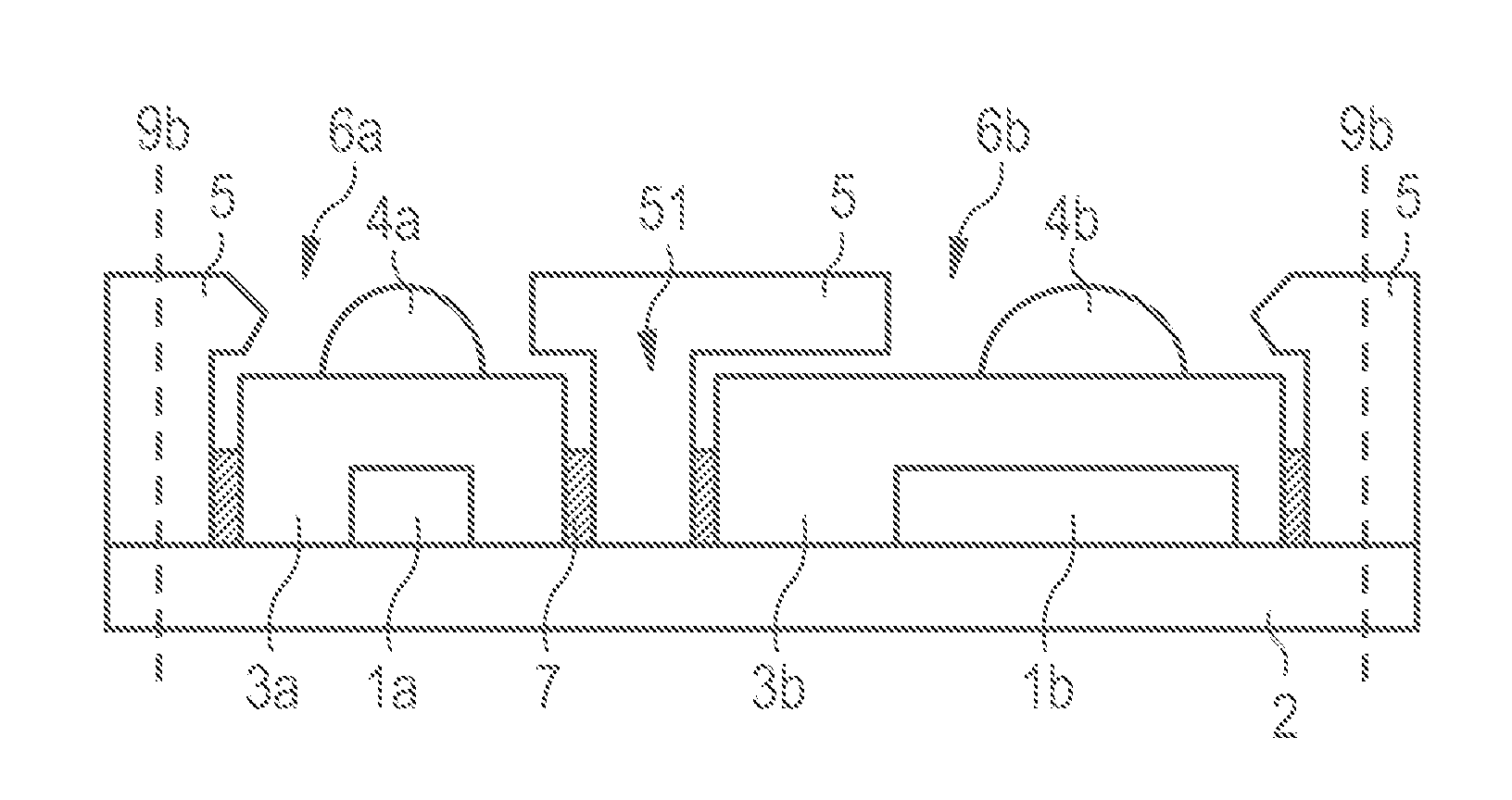
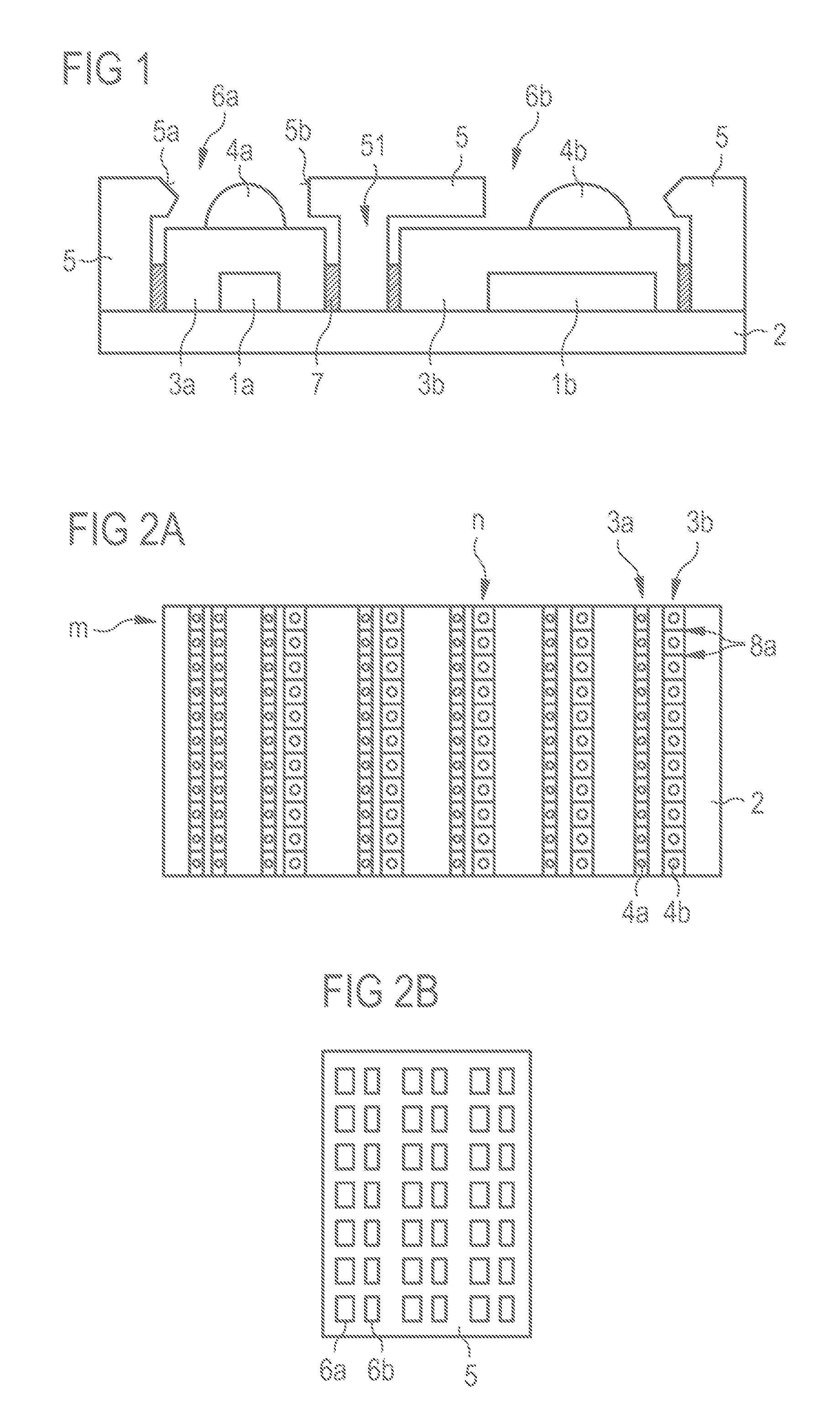
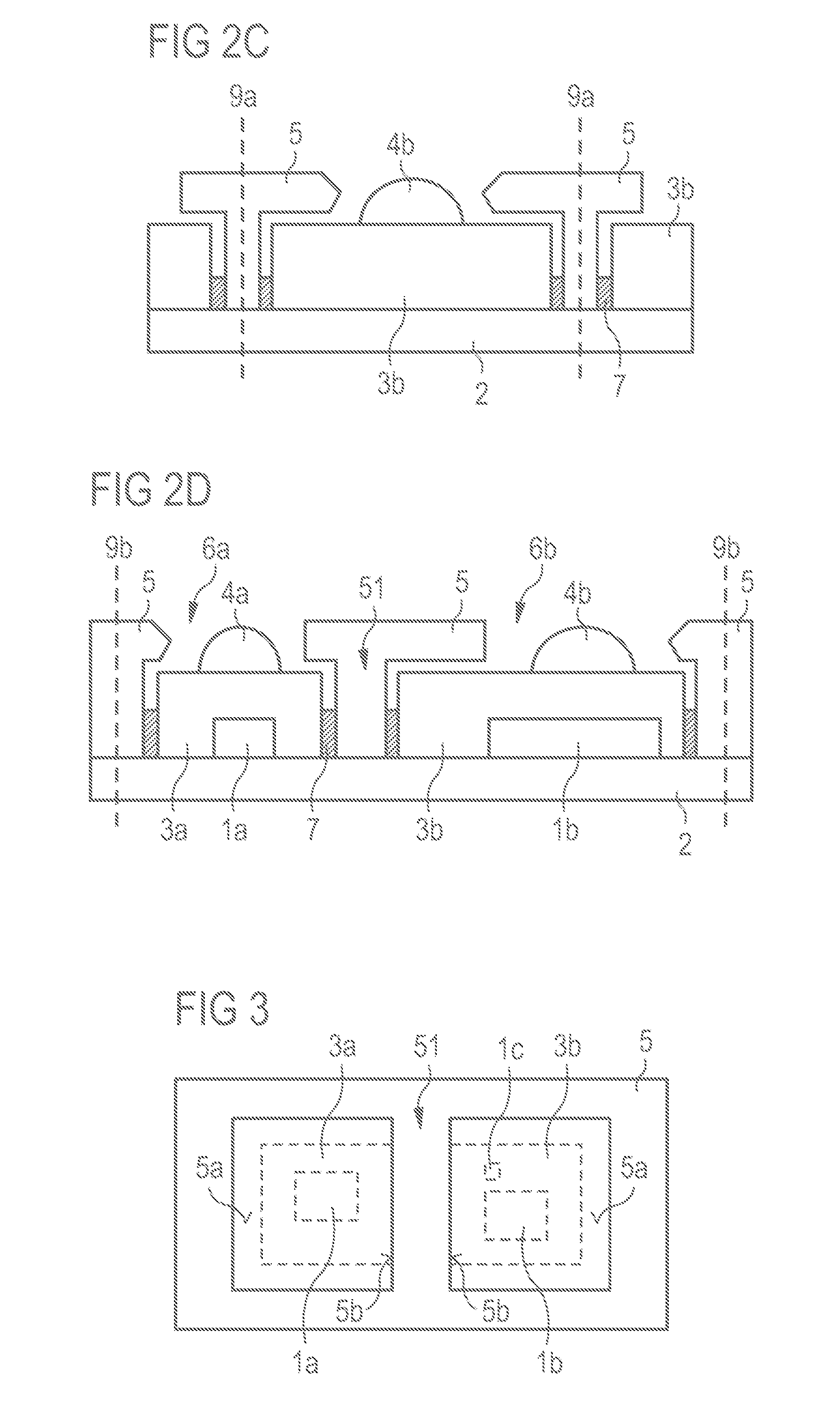
[0048]FIG. 1 shows a cross section of a semiconductor component comprising a carrier substrate 2, on which a radiation-emitting semiconductor chip 1a and a radiation-detecting semiconductor chip 1b are arranged and electrically connected to, for example, conductor tracks on the carrier substrate. In this case, the semiconductor chips 1a, 1b are arranged in a manner laterally spaced apart from one another on the carrier substrate 2.

[0049]The radiation-emitting semiconductor chip 1a has an active layer suitable for generating radiation. By way of example, the radiation-emitting semiconductor chip 1a is an LED which emits radiation in the infrared wavelength frame. The radiation-detecting semiconductor chip 1b has an active layer suitable for detecting radiation and is, for example, a light sensor suitable for detecting radiation in the infrared wavelength range.

[0050]The carrier substrate 2 is, for example, a circuit board, preferably a PCB (printed circuit board).

[0051]The radiation-...


PUM


Abstract

A method for producing a plurality of optoelectronic semiconductor components in combination is specified. A plurality of radiation-emitting and radiation-detecting semiconductor chips are applied on a carrier substrate. The semiconductor chips are potted with a respective potting compound. The potting compounds are subsequently severed by sawing between adjacent semiconductor chips. A common frame is subsequently applied to the carrier substrate The common frame has a plurality of chambers open toward the top. The frame is arranged in such a way that a respective semiconductor chip is arranged in a respective chamber of the frame. A semiconductor component produced in such a way and the use of the semiconductor component are furthermore specified.

Description

[0001]This patent application is a national phase filing under section 371 of PCT / EP2012 / 062009, filed Jun. 21, 2012, which claims the priority of German patent application 10 2011 105 374.7, filed Jun. 22, 2011, each of which is incorporated herein by reference in its entirety.TECHNICAL FIELD[0002]The invention relates to a method for producing a plurality of optoelectronic semiconductor components in combination, each having a radiation-emitting semiconductor chip, a radiation-detecting semiconductor chip and a frame, and to a semiconductor component produced in such a way, and to the use of said semiconductor component.BACKGROUND[0003]Conventionally, semiconductor components having a radiation-emitting semiconductor chip and a radiation-detecting semiconductor chip are usually not produced in combination. By way of example, although conventionally a plurality of semiconductor chips are applied on a common carrier substrate, the carrier substrate is singulated to form individual s...

Claims


Application Information

Patent Timeline
Patent Type & Authority Applications(United States)
IPC IPC(8): H01L31/173H01L31/0203
CPCH01L31/0203H01L31/173G01S7/4813H01L25/167H01L31/167H01L33/486H01L33/54H01L2924/0002H01L2924/00H01L25/16G01S7/481G01S17/08
Inventor LERMER, MARKUSHAUSHALTER, MARTIN
Owner OSRAM OLED
Why Eureka
Try Eureka