
Method for fabricating micro light-emitting diode display

a technology of light-emitting diodes and display panels, which is applied in the direction of semiconductor devices, semiconductor/solid-state device testing/measurement, electrical equipment, etc., can solve the problems of reducing manufacturing yields, increasing costs, and manufacturing displays

Active Publication Date: 2020-12-10
PLAYNITRIDE DISPLAY CO LTD
View PDF0 Cites 4 Cited by
  • Summary
  • Abstract
  • Description
  • Claims
  • Application Information

AI Technical Summary

Benefits of technology

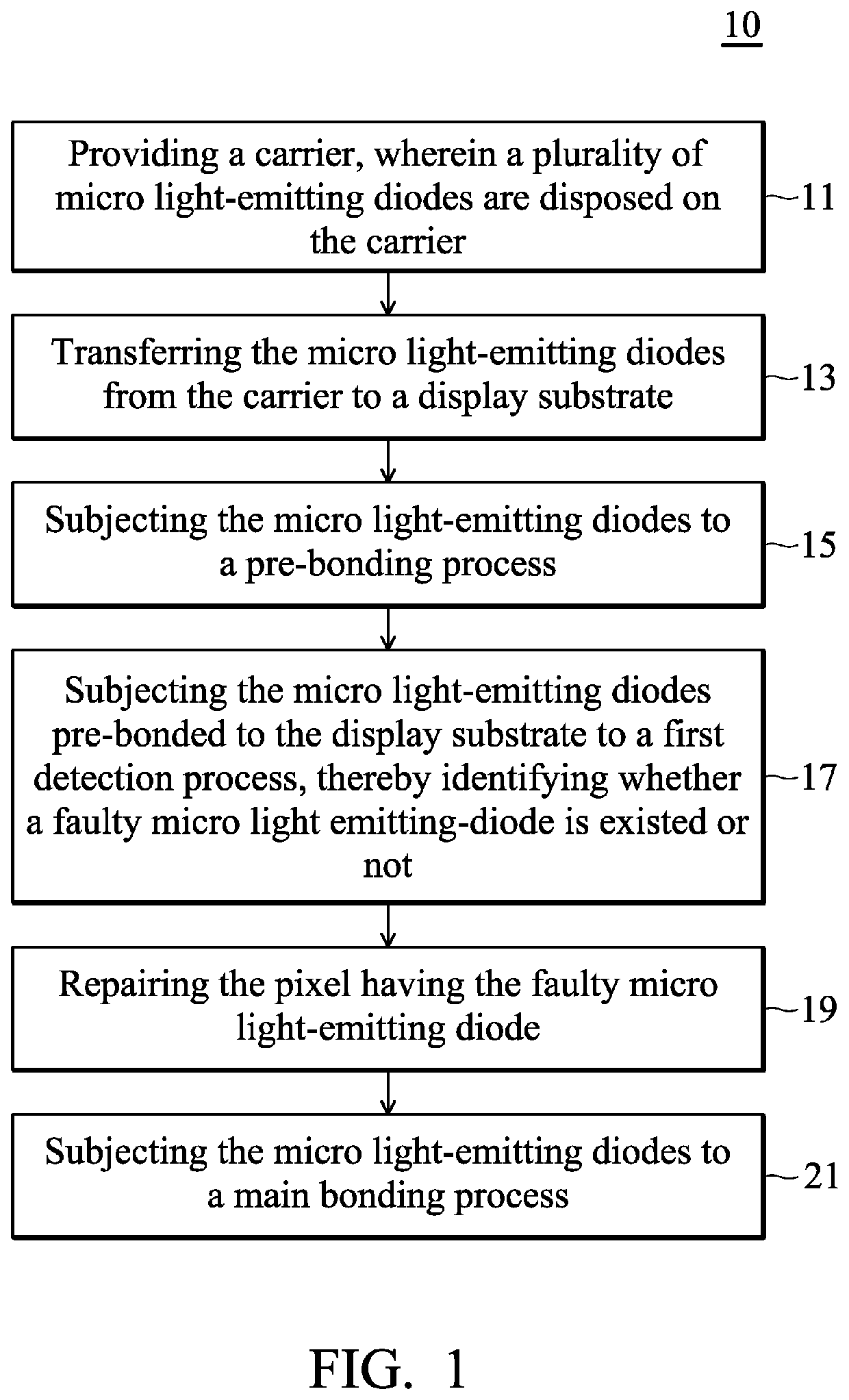
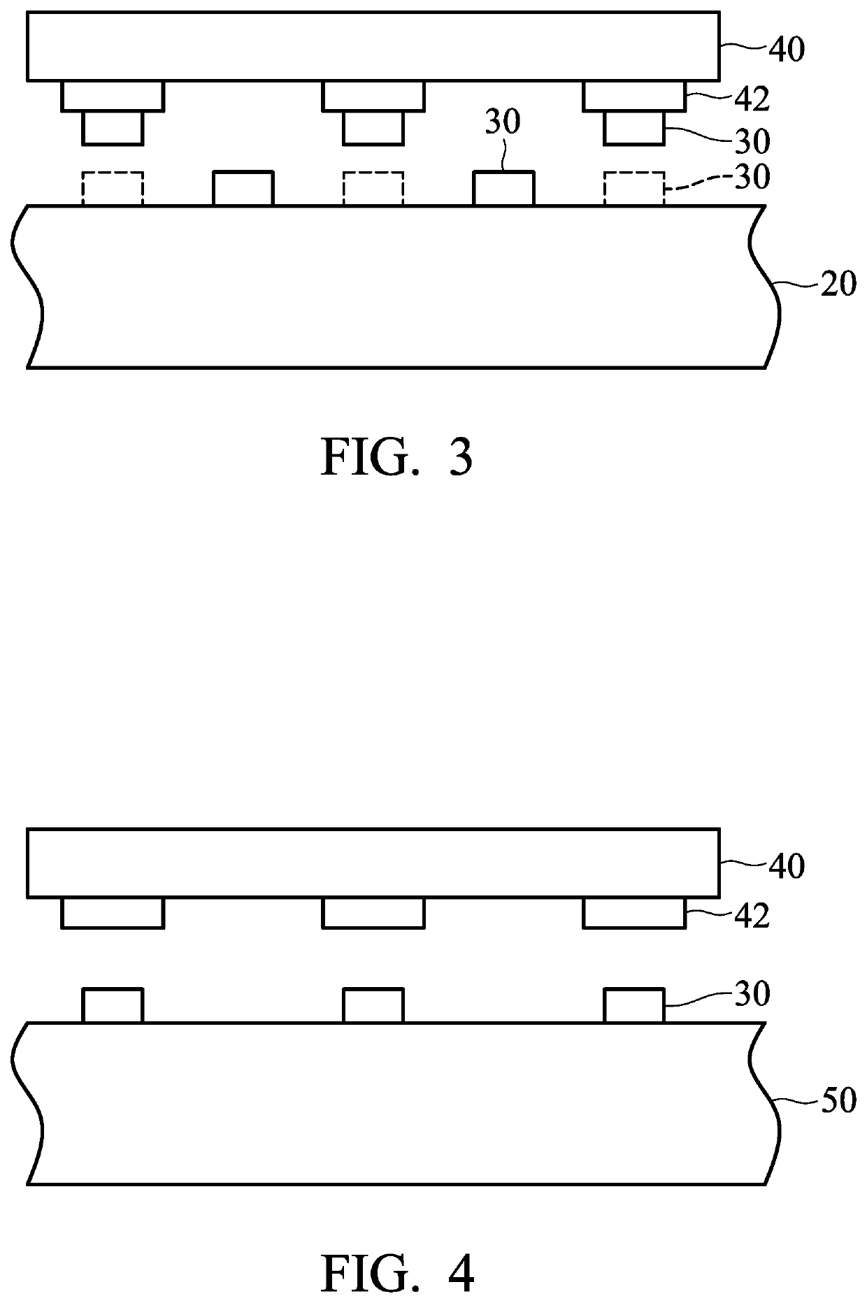
The patent describes a method for making a micro light-emitting diode display by transferring micro light-emitting diodes to a display substrate and bonding them in a pre-bonding process. The method can identify any faulty micro light-emitting diodes and repair them by replacing or disconnecting them. The pre-bonding process has lower bonding strength than the main bonding process but higher process pressure and a shorter process period. The method can also use optical or electrical detection to identify good micro light-emitting diodes for transfer to the display substrate. The technical effects of this patent include improving the yield and reliability of micro light-emitting diode displays.

Problems solved by technology

As display size and resolution increase, it becomes more difficult to manufacture displays without any pixel defects and therefore manufacturing yields decrease and costs increase.

Method used


Image

  • Method for fabricating micro light-emitting diode display
  • Method for fabricating micro light-emitting diode display
  • Method for fabricating micro light-emitting diode display

Examples


Embodiment Construction

[0031]The micro light-emitting diode display of the disclosure is described in detail in the following description. In the following detailed description, for purposes of explanation, numerous specific details and embodiments are set forth in order to provide a thorough understanding of the present disclosure. The specific elements and configurations described in the following detailed description are set forth in order to clearly describe the present disclosure. It will be apparent, however, that the exemplary embodiments set forth herein are used merely for the purpose of illustration, and the inventive concept may be embodied in various forms without being limited to those exemplary embodiments. In addition, the drawings of different embodiments may use like and / or corresponding numerals to denote like and / or corresponding elements in order to clearly describe the present disclosure. However, the use of like and / or corresponding numerals in the drawings of different embodiments d...


PUM


Abstract

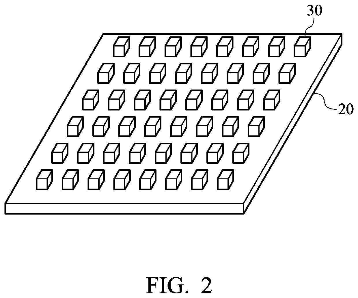
A method for fabricating a micro light-emitting diode display is provided. The method includes disposing a plurality of micro light-emitting diodes on a carrier; transferring the micro light-emitting diodes from the carrier to a display substrate and disposing the micro light-emitting diodes in a plurality of pixels of the display substrate; subjecting the micro light-emitting diodes to a pre-bonding process to electrically connect the micro light-emitting diodes to the display substrate; subjecting the micro light-emitting diodes pre-bonded to the display substrate to a first detection process, thereby identifying whether a faulty micro light-emitting diode is present or not; and, subjecting the micro light-emitting diodes to the main bonding process after the first detection process.

Description

CROSS REFERENCE TO RELATED APPLICATIONS[0001]This Application claims priority of Taiwan Patent Application No. 108119634, filed on Jun. 6, 2019, the entirety of which is incorporated by reference herein.BACKGROUNDField of the Disclosure[0002]The present disclosure relates to a method for fabricating a micro light-emitting diode display.Description of the Related Art[0003]With the advancements being made in the field of optoelectronic technology, the size of optoelectronic components has gradually evolved toward miniaturization. In recent years, due to breakthroughs in the size of light-emitting diodes (LEDs), the micro light-emitting diodes (micro LED) display, in which the micro LEDs are arranged in an array, has increasingly interested people in the field. A micro LED display is a self-luminous display, and it is more energy efficient than organic light-emitting diode (OLED) displays. Furthermore, a micro LED display has better contrast performance than an OLED display, and it is ...

Claims


Application Information

Patent Timeline
IPC IPC(8): H01L33/62H01L21/683H01L21/66H01L25/075
CPCH01L2933/0066H01L22/22H01L33/62H01L25/0753H01L21/6835H01L2221/68368H01L22/14H01L22/12H01L22/20H01L33/0095
Inventor CHEN, YI-CHINGCHEN, PEI-HSINSHIH, YI-CHUNLIN, TZU-YANGLAI, YU-HUNG
Owner PLAYNITRIDE DISPLAY CO LTD
Learn More