Semiconductor device and mounting structure thereof

a technology of semiconductor devices and mounting structures, which is applied in the direction of semiconductor devices, semiconductor/solid-state device details, electrical devices, etc., can solve the problems of difficult to expand the heat dissipation area the difficulty of expanding the heat sink land on the surface of the wiring substrate, so as to achieve the effect of a larger width dimension

Pending Publication Date: 2020-12-24
ROHM CO LTD
View PDF5 Cites 0 Cited by
  • Summary
  • Abstract
  • Description
  • Claims
  • Application Information

AI Technical Summary

Benefits of technology

[0008]According to the present invention, the mounting portion mounted with the semiconductor element is connected to the first terminal portions by the connecting portions having a larger width dimension. Because a part of each first terminal portion is exposed from the sealing resin, the exposed parts of the first terminal portions may be connected to the lands on the wiring substrate when the semiconductor device is mounted on the wiring substrate. Thus, the semiconductor device of the present invention is capable of release heat emitted by the semiconductor device to the lands connected to first terminal portions on the wiring substrate via the connection portion. The lands connected to the first terminal portions may be expanded to a region closer to an outer side than a region surrounded by the lands connected to the second leads. Therefore, the semiconductor device of the present invention ensures the heat dissipation area on the surface of the mounted wiring substrate.

Problems solved by technology

Thus, it would be difficult to expand the heat sink land on the surface of the wiring substrate, or to arrange wires for connecting the electrode pad lands around the heat sink land to the heat sink land.
That is to say, it would be difficult to expand the heat dissipation area on the surface of the wiring substrate, in a way that an area sufficient for thorough heat dissipation cannot be ensured on the surface of the wiring substrate.

Method used


Image

  • Semiconductor device and mounting structure thereof
  • Semiconductor device and mounting structure thereof
  • Semiconductor device and mounting structure thereof

Examples


first embodiment

(First Embodiment)

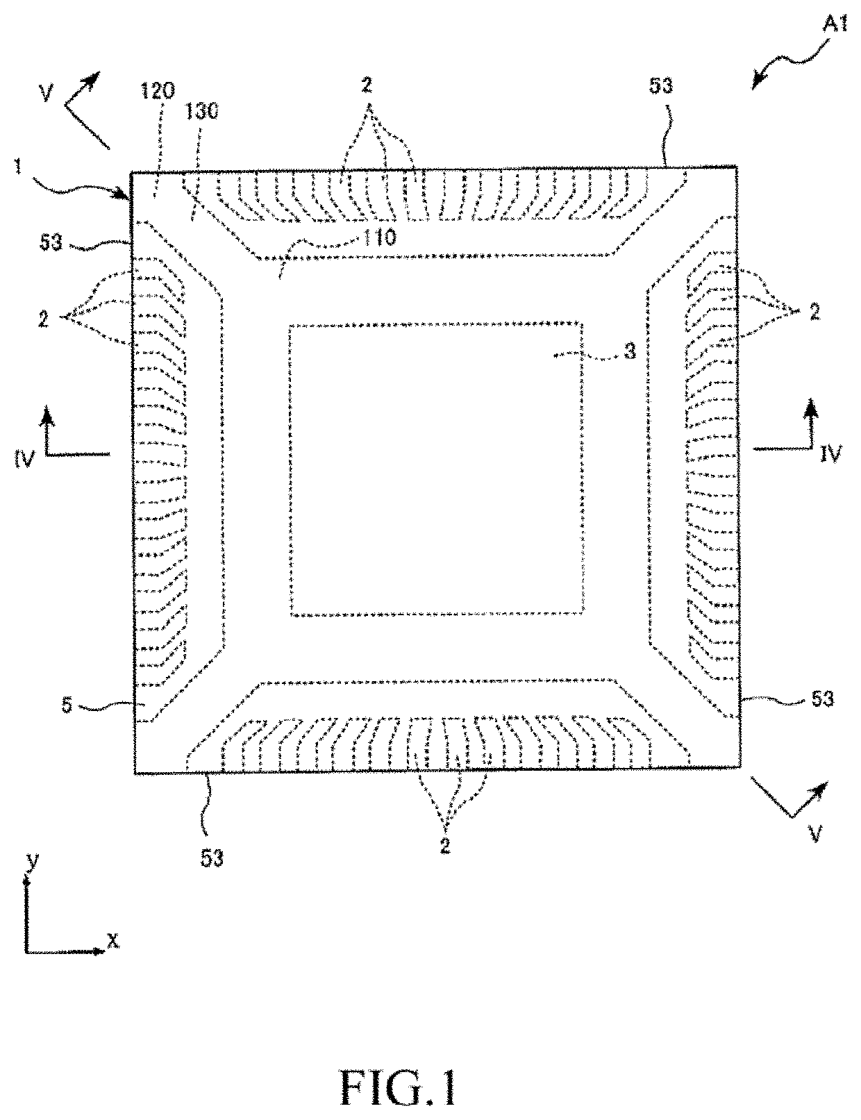
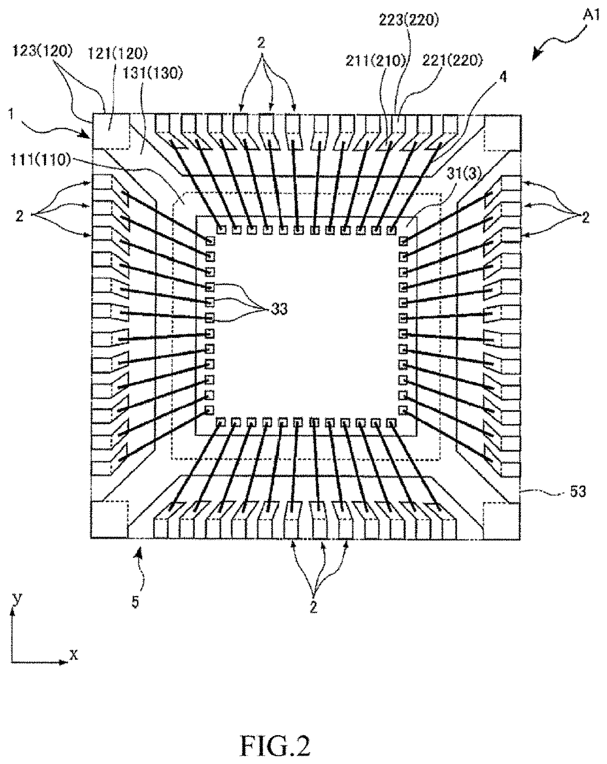
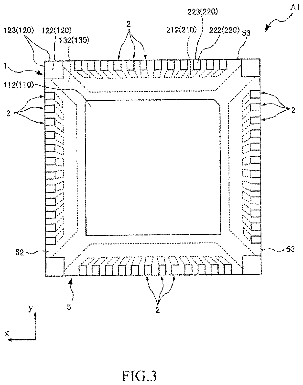
[0028]A semiconductor device A1 according to the first embodiment of the present invention is described with reference to FIG. 1 to FIG. 6. The semiconductor device A1 includes a first lead 1, second leads 2, a semiconductor element 3, bonding wires 4 and a sealing resin 5. The semiconductor device A1 is in a so-called quad flat non-leaded (QFN) package.

[0029]FIG. 1 shows a top view of the semiconductor device A1. FIG. 2 shows a top view of a main part of the semiconductor device A1. FIG. 3 shows a bottom view of the semiconductor device A1. FIG. 4 shows a section diagram of FIG. 1 along the line IV-IV. FIG. 5 shows a section diagram of FIG. 1 along the line V-V. FIG. 6 shows an enlarged top view of the main part. In FIG. 2 and FIG. 6, for better understanding, an imaginary line (double-dotted line) is used for the sealing resin 5 to indicate the contour of the sealing resin 5.

[0030]The semiconductor device A1 in these drawings is a device that is surface mounted o...

second embodiment

(Second Embodiment)

[0070]A semiconductor device A2 according to the second embodiment of the present invention is described with reference to FIG. 13 and FIG. 14. In these drawings, components identical or similar to those of the semiconductor device A1 are denoted by the same numerals, and repeated details are omitted.

[0071]FIG. 13 shows a bottom view of the semiconductor device A2, and is a drawing corresponding to FIG. 3 of the first embodiment. FIG. 14 shows an enlarged section diagram of a main apart of a state in which the semiconductor device A2 is mounted on the wiring substrate 9, and is a drawing corresponding to FIG. 8 of the first embodiment.

[0072]The semiconductor device A2 of this embodiment differs from the semiconductor device A1 in that, the mounting portion back surfaces 112 are not exposed from the sealing resin 5. The mounting portion 110 of this embodiment has a thickness (the dimension in the z direction) equal to the thickness of the connecting portions 130, a...

third embodiment

(Third Embodiment)

[0074]A semiconductor device A3 according to the third embodiment of the present invention is described with reference to FIG. 15 and FIG. 16. In these drawings, components identical or similar to those of the semiconductor device A1 are denoted by the same numerals, and repeated details are omitted.

[0075]FIG. 15 shows a bottom view of the semiconductor device A3, and is a drawing corresponding to FIG. 3 of the first embodiment. FIG. 16 shows an enlarged section diagram of a main apart of a state in which the semiconductor device A3 is mounted on the wiring substrate 9, and is a drawing corresponding to FIG. 8 of the first embodiment.

[0076]The semiconductor device A3 of this embodiment differs from the semiconductor device A1 in that, the connecting portion back surfaces 132 are exposed from the sealing resin 5. The connecting portions 130 of this embodiment have a thickness (the dimension in the z direction) is equal to the thickness of the mounting portion 110 an...


PUM

PropertyMeasurementUnit
widthaaaaaaaaaa
thicknessaaaaaaaaaa
thicknessaaaaaaaaaa

Abstract

A semiconductor device includes a semiconductor element, a first lead (1), a plurality of second leads and a sealing resin. The first lead includes a mounting portion mounting the semiconductor element, four connecting portions extending from four corners of the mounting portion, respectively, and four first terminal portions connected to front ends of the connecting portions, respectively. A part of each first terminal portion is exposed from the sealing resin. The second leads are arranged in a plural quantity between adjacent first terminal portions when viewed in a thickness direction. Each second lead includes a second terminal portion having a part exposed from the sealing resin, and a joining portion extending from the second terminal portion toward the mounting portion. A connecting portion width dimension of the connecting portion is greater than a joining portion width dimension of the joining portion of the second lead adjacent to the connecting portion.

Description

FIELD OF THE INVENTION[0001]The present invention relates to a semiconductor device and a mounting structure of the semiconductor device.DESCRIPTION OF THE PRIOR ART[0002]Semiconductor devices in quad flat non-leaded (QFN) packages have been developed as surface-mounted semiconductor devices on wiring substrates. Patent publication 1 discloses an example of a QFN semiconductor device. In a QFN semiconductor device, a plurality of electrode pads are disposed along four side surfaces, respectively. Further, a semiconductor device having a heat sink for releasing heat emitted from a semiconductor element is disposed on a back surface of the QFN semiconductor device.[0003]FIG. 17 shows a bottom view of such conventional semiconductor device A100. The semiconductor device A100 exposes, from the back surface of the sealing resin 5, a first lead mounted with a semiconductor device. When the semiconductor device A100 is mounted on a wiring substrate, the back surface of the first lead 1 is ...

Claims


Application Information

Patent Timeline
Patent Type & Authority Applications(United States)
IPC IPC(8): H01L23/498H01L23/00H01L23/31
CPCH01L24/45H01L23/49838H01L23/49861H01L23/3121H01L23/49811H01L21/4821H01L23/49541H01L23/49568H01L23/3107H01L23/49548H01L23/49503H01L2224/48245H01L2224/32245H01L2224/49173H01L24/48H01L2224/73265H01L2224/45147H01L2224/85455H01L2224/85447H01L2224/83447H01L2224/8546H01L2224/45124H01L2224/83455H01L2224/29099H01L2224/85444H01L2224/8346H01L2224/83444H01L2224/45144H01L2224/48247H01L2924/18301H01L2924/00014H01L2924/013H01L2924/01404H01L2924/00012H01L21/4825H01L21/4853
Inventor YASUTAKE, IPPEI
Owner ROHM CO LTD
Why Eureka
Try Eureka