Lead frame

a lead frame and lead wire technology, applied in the field of lead frames, can solve the problems of lowering the connection of the bonding wire w with respect to the grounding lead fa, and achieve the effects of preventing the connection of the bonding wire, reducing the wear of the dicing blade, and sufficient supporting properties

Active Publication Date: 2018-03-06
MITSUI HIGH TEC INC
View PDF14 Cites 0 Cited by
  • Summary
  • Abstract
  • Description
  • Claims
  • Application Information

AI Technical Summary

Benefits of technology

[0016]In consideration with the above, the present invention is directed to a lead frame for manufacturing a semiconductor apparatus in the MAP scheme. An object of the present invention is to provide a lead frame to achieve an enhancement of a connectivity of a bonding wire with respect to a grounding lead by preventing a deformation of the grounding lead in wire bonding in advance.
[0021]According to the lead frame of the first aspect of the present invention, the grounding leads extended from the adjacent die pads are aligned on a common axis while providing the connecting bar between the grounding leads, and a support projection is provided at the one surface on the connecting bar in the common axis. Accordingly, even if the grounding leads and the connecting bar are formed to be thinned by half etching from the one surface side, the support projection which is provided on the one side of the connecting bar functions as a support when the bonding wire is connected to the grounding lead on the working stage. Thus, the grounding leads are hardly bent and deformed downwards due to the depression force generated when an end of the bonding wire is connected, thereby preventing a connectivity of the bonding wire with respect to the grounding lead from lowered in advance.
[0022]According to the lead frame of the second aspect of the present invention, the width dimension of the support projection in the connecting bar is the same as the width dimension of the connecting bar. Thus, it is possible to secure the sufficient supporting property due to the existence of the support projection and possibly suppress a wear of a dicing blade.
[0023]According to the lead frame of the third aspect of the present invention, the width dimension of the support projection in the connecting bar is larger than the width dimension of the connecting bar and smaller than the width dimension of the dicing line. Thus, it is possible to secure the better sufficient supporting property due to the existence of the support projection while the suppression of the wear of the dicing blade is slightly deteriorated.
[0024]According to the lead frame of the fourth aspect of the present invention, the width dimension of the support projection in the grounding lead is the same as the width dimension of the grounding lead. Thus, it is possible to secure the sufficient supporting property due to the existence of the support projection and possibly suppress the wear of the dicing blade.

Problems solved by technology

After the semiconductor chips C are bonded on the die pad Fd of the lead frame LF on a working stage S as shown in FIG. 8A, the bonding wires W are connected to the grounding leads Fa, Fa of the lead frame LF on the working stage S. In this case, as shown in FIG. 8B, because no supports exist on the rear side, the grounding leads Fa, Fa are bent and deformed downwards due to the depression force f, f generated when ends of the bonding wires W are connected, thereby raising a problem that a connectivity of the bonding wire W with respect to the grounding lead Fa is lowered.

Method used


Image

  • Lead frame
  • Lead frame
  • Lead frame

Examples


Embodiment Construction

[0038]A lead frame according to an exemplary embodiment of the present invention will be described in detail with reference to accompanying drawings.

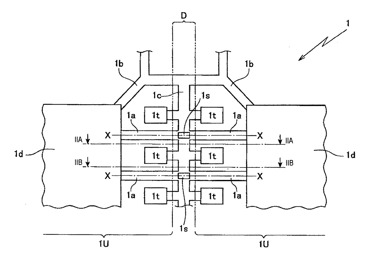
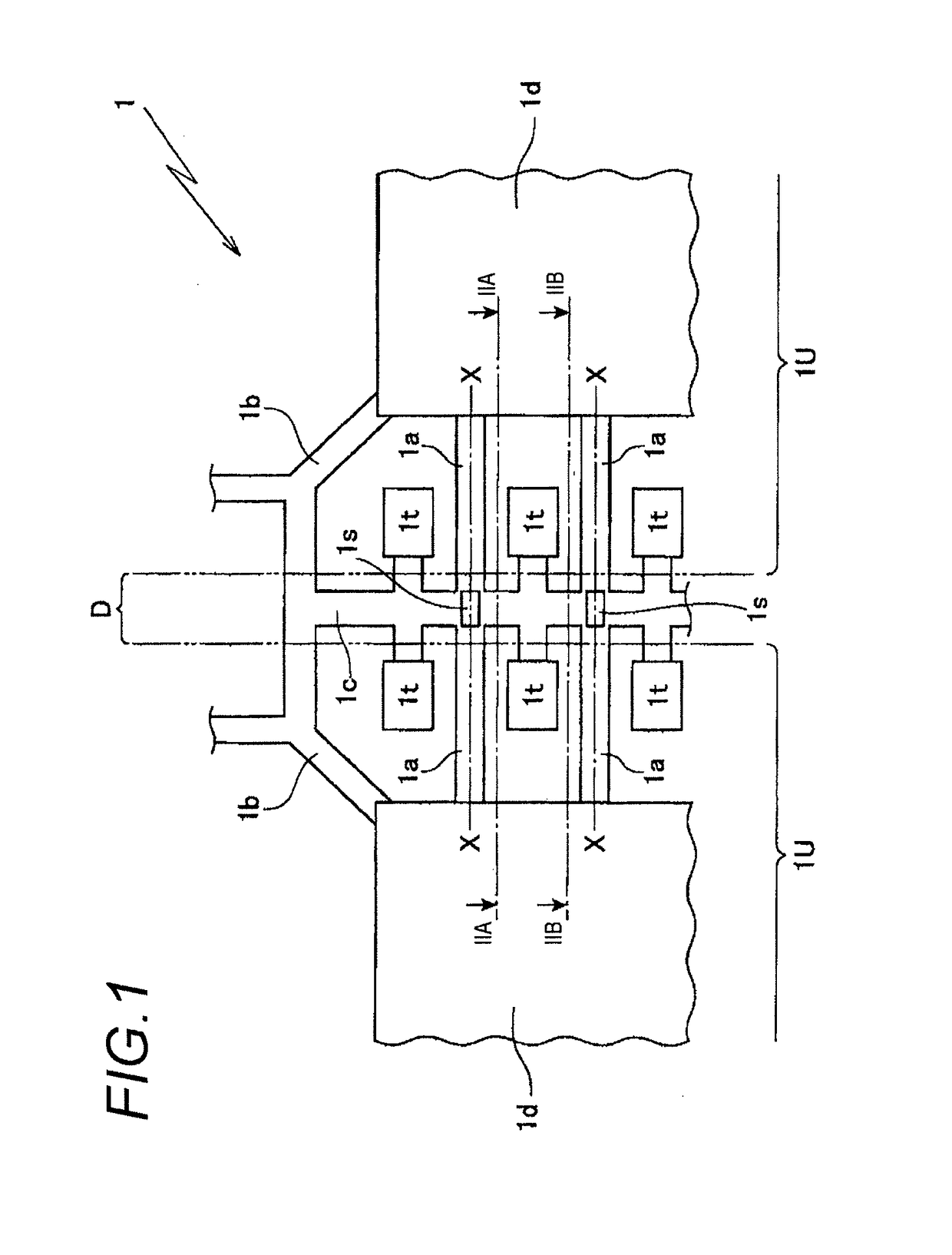
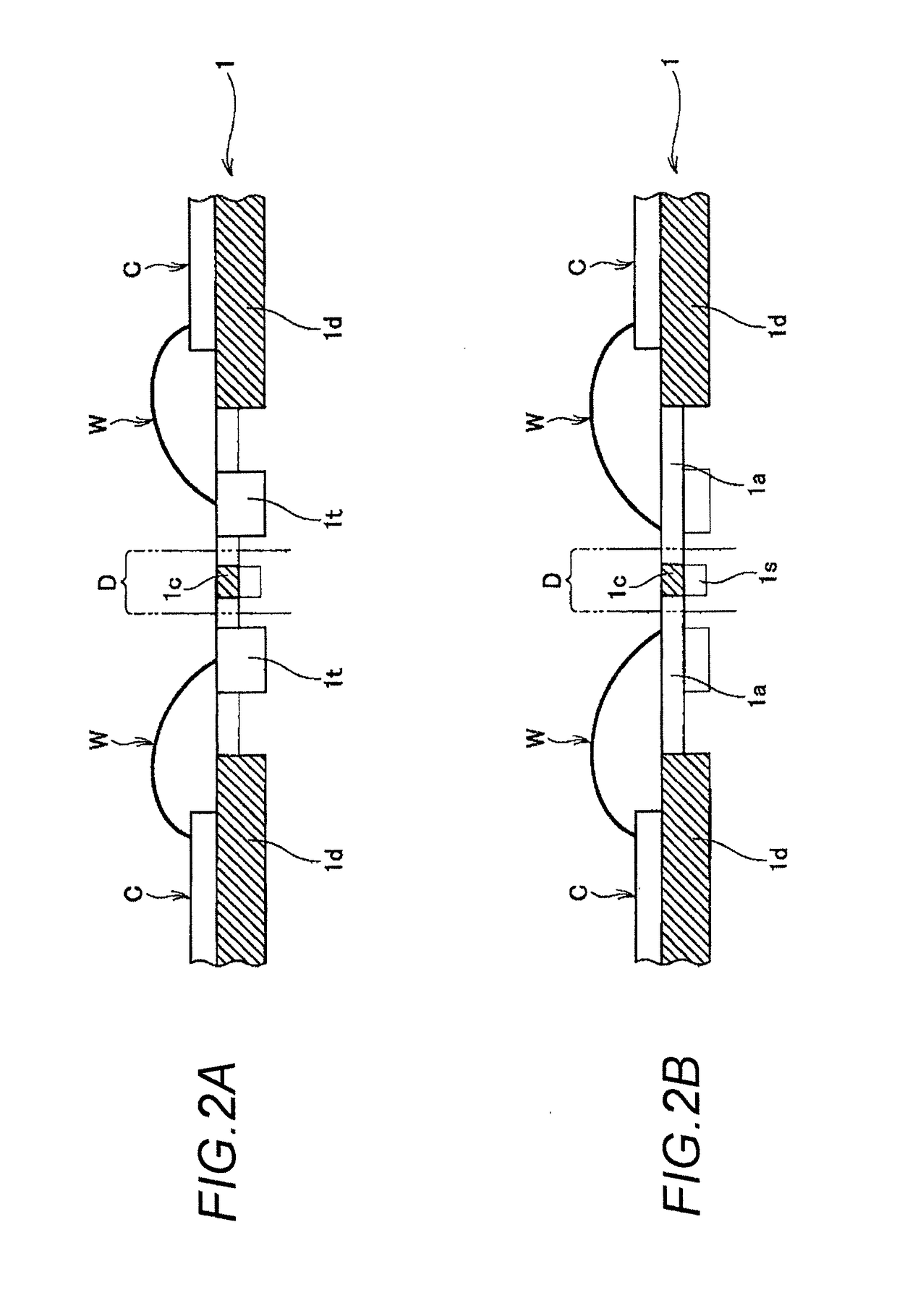
[0039]FIGS. 1, 2A and 2B show a lead frame according to an embodiment of the present invention for manufacturing a QFN package (Quad Flat Non-leaded Package) as a form of a semiconductor apparatus in a MAP (Molded Array Process) scheme.

[0040]A lead frame 1 according to the embodiment include a plurality of unit lead frames 1U, 1U, . . . arranged in a matrix. Each of the unit lead frames 1U includes a die pad 1d having a rectangular shape, and a plurality of external electrode terminals (terminal leads) 1t, 1t, . . . arranged around the die pad 1d.

[0041]A grounding lead 1a is integrally formed and extended from the die pad1d of each unit lead frame 1U. The grounding leads 1a, 1a, which are extended respectively from the adjacent die pads 1d, 1d in the adjacent unit lead frames 1U, 1U, are interconnected via a connecting bar 1c. The conn...


PUM


Abstract

A lead frame includes adjacent die pads which lie adjacent to each other; grounding leads extended from the adjacent die pads; a connecting bar by which the grounding leads extended from the adjacent die pads are interconnected. The grounding leads and the connecting bar are formed to be thinner at one surface than a maximum thickness of leads of the lead frame, the grounding leads extended from the adjacent die pads are aligned on a common axis while providing the connecting bar between the grounding leads, and a support projection is provided at the one surface on the connecting bar in the common axis.

Description

CROSS-REFERENCE TO RELATED APPLICATIONS[0001]This application is based upon and claims the benefit of priority of Japanese Patent Application No. 2013-002599 filed on Jan. 10, 2013, the contents of which are incorporated herein by reference in its entirety.BACKGROUND OF THE INVENTION[0002]1. Field of the Invention[0003]The present invention is directed to a lead frame for manufacturing a semiconductor apparatus by a MAP (Molded Array Process) scheme, and relates to a lead frame in which grounding leads which are extended from adjacent die pads are interconnected via a connecting bar.[0004]2. Description of the Related Art[0005]Recently, when a QFN package (Quad Flat Non-leaded Package) as one form of a semiconductor apparatus is manufactured, it is promoted to adopt a MAP (Molded Array Process) scheme in which a plurality of semiconductor chips are collectively sealed on a lead frame, and then individual semiconductor apparatuses are individualized by dicing.[0006]Even for a lead fr...

Claims


Application Information

Patent Timeline
Patent Type & Authority Patents(United States)
IPC IPC(8): H05K7/18H01L23/00
CPCH01L24/97H01L2224/48091H01L2224/48247H01L2924/181H01L2924/00014H01L2924/00
Inventor ISHIBASHI, TAKAHIRO
Owner MITSUI HIGH TEC INC
Why Eureka
Try Eureka