Surface acoustic wave device and method of manufacturing the same

a surface acoustic wave and acoustic wave technology, applied in the direction of impedence networks, electrical equipment, piezoelectric/electrostrictive/magnetostrictive devices, etc., can solve the problems that the saw device cannot meet the requirements of miniaturization, the saw device may be unstable, etc., to achieve less parasitic capacitance, reduce the difference, and improve the effect of performan

Active Publication Date: 2021-01-14
CHIPBOND TECH
View PDF5 Cites 0 Cited by
  • Summary
  • Abstract
  • Description
  • Claims
  • Application Information

AI Technical Summary

Benefits of technology

[0005]The object of the present invention is to provide a SAW device having less parasitic capacitance and higher performance by reducing difference between receiving space area of transducer and package area of SAW device.

Problems solved by technology

The more the IDT finger pairs, the bigger the size of the SAW device is required to provide a bigger space for receiving IDT, but increasing SAW device size to improve performance cannot meet requirements of miniaturization.
Besides, the more the IDT finger pairs, the more the heat generated by IDT, the SAW device may be unstable when heat dissipation cannot be achieved sufficiently.

Method used


Image

  • Surface acoustic wave device and method of manufacturing the same
  • Surface acoustic wave device and method of manufacturing the same
  • Surface acoustic wave device and method of manufacturing the same

Examples


Embodiment Construction

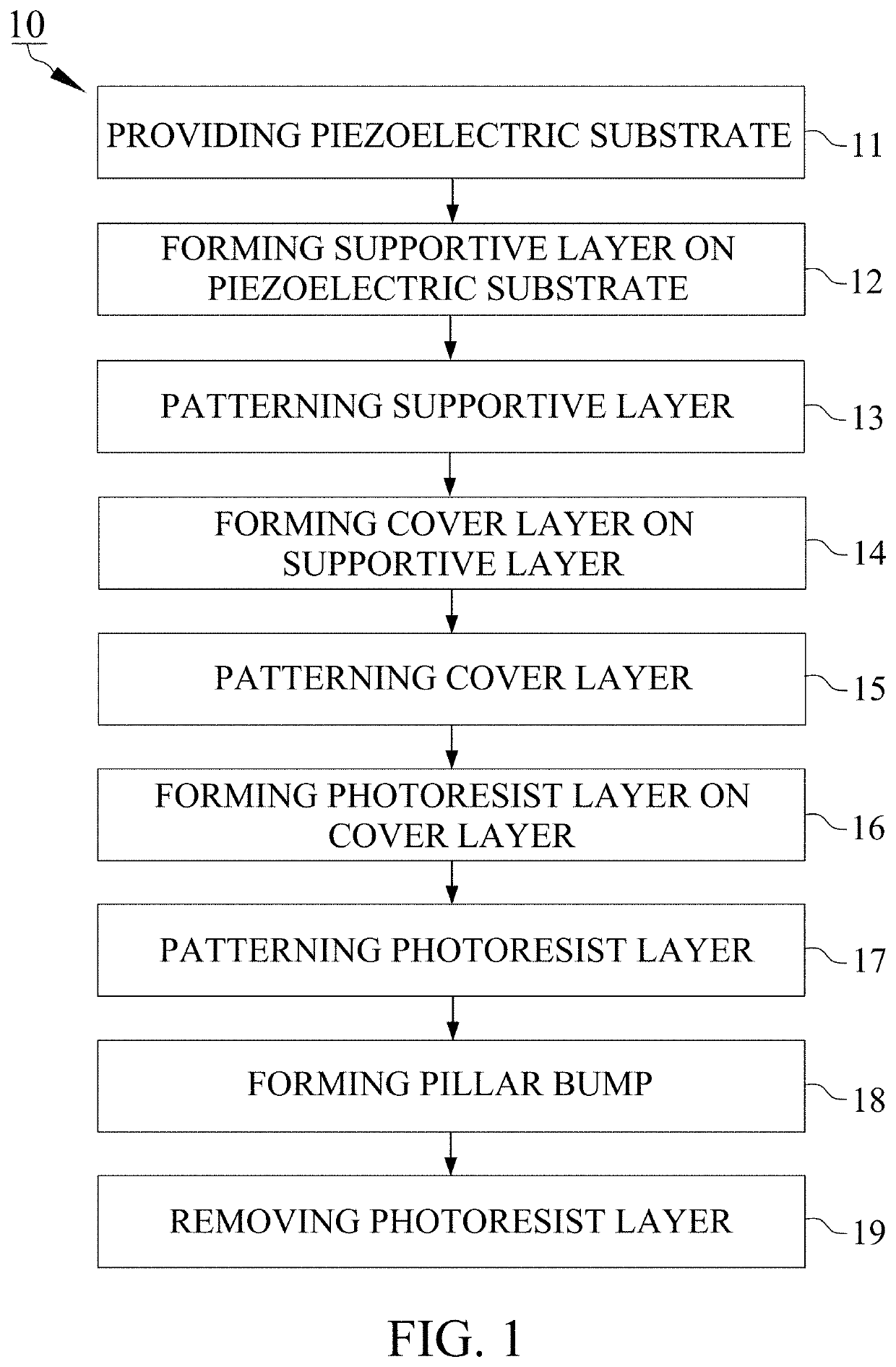
[0024]With reference to FIG. 1, a method 10 of manufacturing a SAW device in accordance with one embodiment of the present invention includes a step 11 of providing piezoelectric substrate, a step 12 of forming supportive layer on piezoelectric substrate, a step 13 of patterning supportive layer, a step 14 of forming cover layer on supportive layer, s step 15 of patterning cover layer, a step 16 of forming photoresist layer on cover layer, a step 17 of patterning photoresist layer, a step 18 of forming pillar bump and a step 19 of removing photoresist layer.

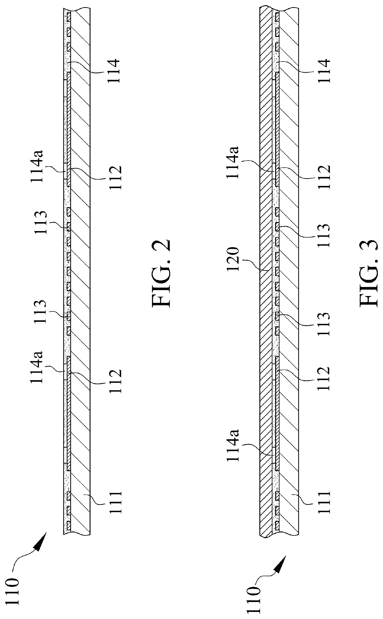
[0025]With reference to FIG. 2, a piezoelectric substrate 110 provided in the step 11 includes a base 111, a conductive pad 112 and a transducer 113. The base 111 is made of piezoelectric material such as quartz, LiTaO3 (LT), LiNbO3 (LN), PbTiO3 (PTO) or Pb(Zr, Ti)O3 (PZT). The conductive pad 112 and the transducer 113 are disposed on a surface of the base 111 and electrically connected with each other. The conductive pad 112 and...


PUM


Abstract

A surface acoustic wave device includes a piezoelectric substrate, a supportive layer, a cover layer and a pillar bump. The supportive layer is disposed on the piezoelectric substrate and around a transducer, the cover layer covers the supportive layer, and the pillar bump is located in a lower via hole of the supportive layer and an upper via hole of the cover layer. The upper via hole has a lateral opening located on a lateral surface of the cover layer, and the pillar bump in the cover layer protrudes from the lateral surface of the cover layer via the lateral opening.

Description

FIELD OF THE INVENTION[0001]This invention relates to a surface acoustic wave (SAW) device, and more particularly to a SAW device having improved frequency response capability.BACKGROUND OF THE INVENTION[0002]FIG. 21 shows a conventional SAW device 200 which includes a piezoelectric substrate 210, a wall 220, a lid 230, a bump 240 and a solder cap 250. The piezoelectric substrate 210 includes a carrier 211, a pad 212 and an interdigital transducer (IDT) 213, the pad 212 and the IDT 213 are mounted on the carrier 211. The wall 220 surrounds the IDT 213 and the lid 230 covers the wall 220 so that the IDT 213 is located in a space between the lid 230 and the piezoelectric substrate 210, the bump 240 is located in a via hole through the wall 220 and the lid 230, and the solder cap 250 is electrically connected to the pad 212 via the bump 240.[0003]The package size of the conventional SAW device 200 is bigger than the space for receiving the IDT 213 due to the bump 240 disposed in the vi...

Claims


Application Information

Patent Timeline
Patent Type & Authority Applications(United States)
IPC IPC(8): H03H9/02H03H9/05H01L41/047H03H9/145
CPCH03H9/02952H03H9/059H03H9/02834H03H9/145H01L41/0477H03H9/02543H03H9/02614H03H9/02669H03H9/1071H03H3/08H03H9/02992H03H9/14538H10N30/877
Inventor SHIH, CHENG-HUNGLIN, CHENG-FAN
Owner CHIPBOND TECH
Why Eureka
Try Eureka