System with logic and embedded MIM capacitor

a technology of logic and capacitors, applied in capacitors, digital storage, instruments, etc., can solve the problems of unintentional parasitic capacitance behavior of logic circuits controlling edrams, affecting signal levels, signal speed, signal integrity, etc., to reduce parasitic capacitance, reduce parasitic capacitance, and reduce the effect of source (s) and drain

Active Publication Date: 2013-11-19
MOSYS INC
View PDF3 Cites 0 Cited by
  • Summary
  • Abstract
  • Description
  • Claims
  • Application Information

AI Technical Summary

Benefits of technology

[0008]An improved method and apparatus for an embedded random access memory (RAM) system with a metal-insulator-metal (MIM) capacitor is achieved. The RAM system of the present disclosure has an embedded memory and a logic circuit on the same substrate. The RAM can be either dynamic RAM (DRAM) or static RAM (SRAM), e.g., 6-transistor (6-T) cell. In particular, a MIM capacitor can be used in a DRAM cell as a storage capacitor and in a SRAM cell to improve the soft error rate (SER).
[0011]Thus, the present disclosure reduces parasitic capacitance between the source contacts and the drain contacts of the logic transistors, which are more sensitive to switching speeds than memory transistors, by having one or more metal layers located as close to the source / drain contacts as possible, e.g., below the top surface of the MIM capacitor. The more source and drain contacts per transistor, e.g., three contacts for each source and three contacts for each drain for a given transistor, and the closer the source is to the drain, e.g., for smaller size and to minimize the effect of source (S) and drain (D) resistance, then the more they act as a plate capacitor. By keeping the contacts short, e.g., by using the metal layer as low in the layer structure as possible, the less the parasitic capacitance created between the source and the drain contacts. By communicating signals to upper metal layers using via plugs, coupled to the metal layer, that are fewer in number and that are spaced farther apart from each other than the source and drain contacts, the less the parasitic capacitance in the system compared to using the contacts to reach an upper metal layer. By reducing the parasitic capacitance of the system, the RC time constant is correspondingly reduced, which then increases the switching speed of the logic transistor.
[0012]Furthermore, by co-locating the one or more metal layers with the MIM capacitor, e.g., above the bottom surface of the MIM capacitor, or at the same layer heights as the MIM capacitor, the overall structure of MIM capacitor and metal layers is shorter, compared to an alternative embodiment of locating the MIM cell above a first metal layer. The result is a shorter contact / via plug height, which reduces the resistance of the circuit, correspondingly reduces the RC time constant, and thereby increases the switching speed of the transistor. While a metal layer can be utilized for a transistor in the memory region adjacent to the MIM capacitor, e.g., below the top surface of the MIM capacitor and above the bottom surface of the MIM capacitor, the memory cell may require wider spacing in order to provide sufficient insulating distance between the metal line and the MIM capacitor. However, by having a metal layer only in the logic region, located at a level below the top surface of the MIM capacitor and above the bottom surface of the MIM capacitor, all the benefits of reduced parasitic capacitance and resistance mentioned herein is achieved, from shorter contacts and fewer via plugs that are spaced further apart than the contacts are achieved, without having a wider memory cell.
[0013]The present disclosure is also directed to a method for forming an embedded DRAM system that includes DRAM cells and logic transistors on a single substrate, where the contacts are formed from different conductive material. The use of two different types of plugs reduces the overall interconnect resistance, because at least one of the plugs is a lower resistance material, which thereby improves system level performance by enhancing the speed and power features of the present disclosure.

Problems solved by technology

These unintended capacitive properties can be referred to as parasitic capacitance, which undesirably affects signal levels, signal speed, and signal integrity.
While an eDRAM system utilizes a specific capacitor device, such as a trench capacitor, or a metal-insulator-metal (MIM) capacitor, built into the semiconductor structure to store a desired charge for a logic level, the logic circuit controlling the eDRAM can unintentionally have parasitic capacitance behavior.

Method used


Image

  • System with logic and embedded MIM capacitor
  • System with logic and embedded MIM capacitor
  • System with logic and embedded MIM capacitor

Examples


fourth embodiment

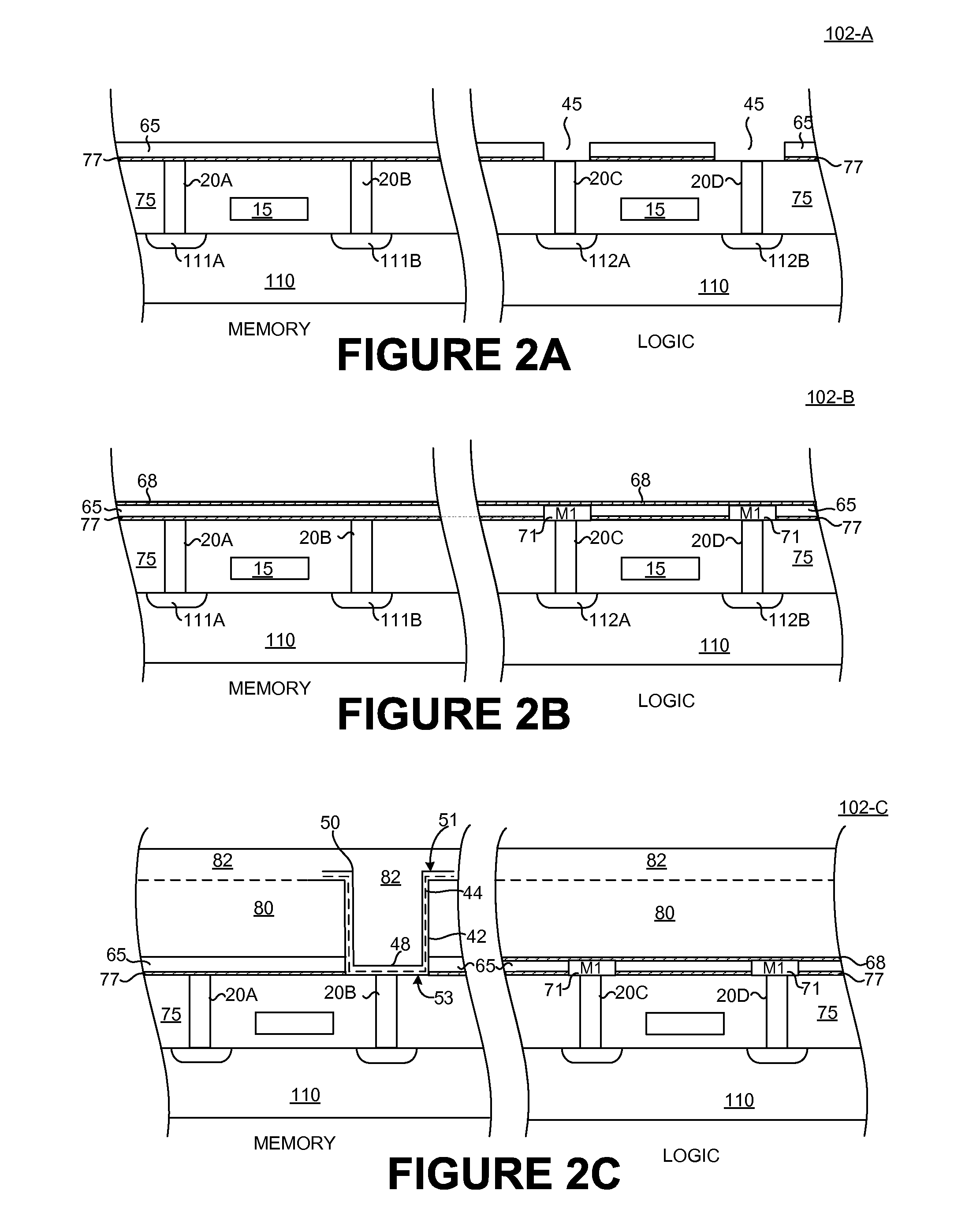
[0038]Referring now to FIG. 4, a cross-sectional view of one portion of a process flow for forming a semiconductor structure 104 having an embedded DRAM system with a first metal layer in the memory region located at a layer corresponding to a location between a top and bottom surface of a MIM capacitor is shown, in accordance with the present disclosure. Semiconductor structure 104 corresponds directly to FIG. 2C with the addition of a metal layer, M1 interconnect 71, located in memory region between a top surface 51 and a bottom surface 53 of MIM capacitor 50, and coupled to drain 111A through contact 20A. Note that a via, similar to 18A of FIG. 3D, is not used in memory section of FIG. 4, because M171 over contact 20A completes the routing for a bit line. Subsequent processing operations for vias and plugs with corresponding conditions is per FIGS. 2D, 3C and 3D, or 5B-5C.

[0039]While using metal layer M1 interconnect 71 in memory region may reduce parasitic capacitance in the mem...

fifth embodiment

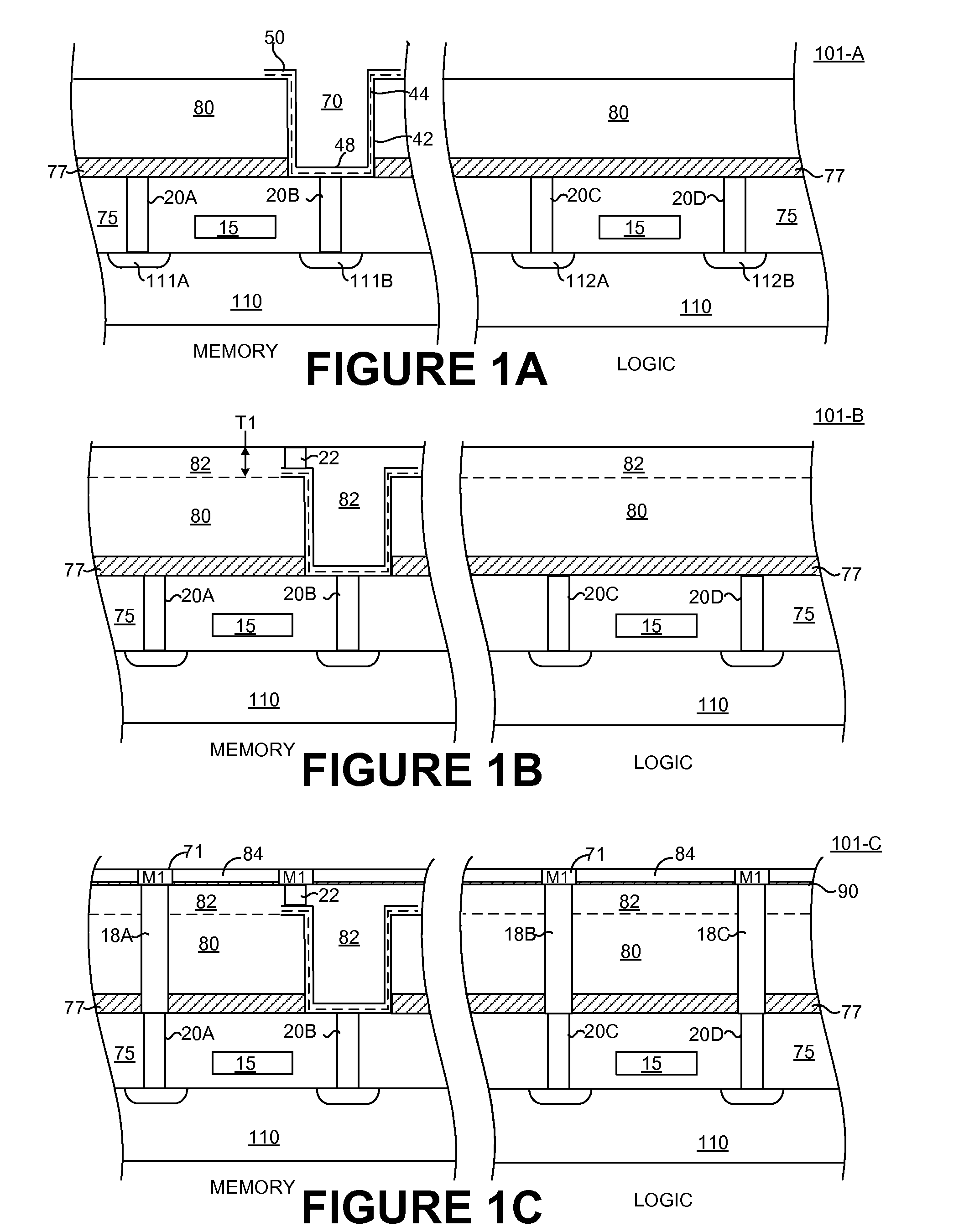
[0040]Referring now to FIGS. 5A-5C, cross-sectional views of a process flow for forming an embedded DRAM system having a MIM capacitor by different sequencing of via formation is shown, in accordance with the present disclosure. Partially completed semiconductor structure 105-A of FIG. 5A is fabricated according to the process described for FIGS. 2A-2C, including the conventional process to form M1 first metal layer 71. While etch-stop layer 68 and dielectric layer 65 are capable of being removed prior to forming dielectric layer 80 for a simplified etching of via 18A, the illustration retains etch-stop layer 68 and dielectric layer 65 in the memory region, except as required for the formation of MIM capacitor 50. To form the MIM capacitor 50, dielectric layers 80 and 65 and etch-stop layers 68 and 77 are etched and MIM capacitor is formed therein as described in FIG. 2C. After completion of the MIM capacitor 50, second dielectric layer 82 is then formed as described in FIG. 2C. In ...

sixth embodiment

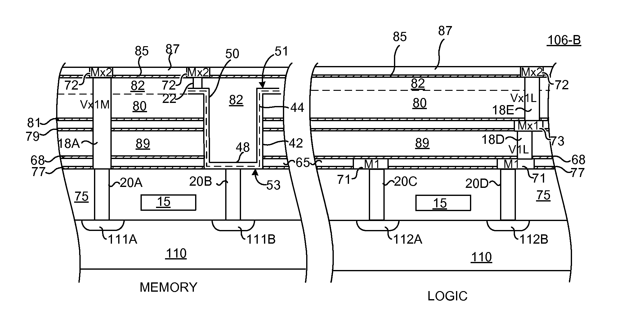
[0042]Referring now to FIGS. 6A-6B, a cross-sectional view of a process flow for forming an embedded DRAM system having multiple metal layers in the logic region located between a top and bottom surface of a MIM capacitor, in accordance with the present disclosure. Partially completed semiconductor structure 106-A of FIG. 6A is fabricated according to the process described for FIGS. 2A-2B, including the conventional processing to form M1 first metal layer 71 in dielectric layer 65, over which is formed second etch-stop layer 68, over which is next disposed first dielectric layer 89. Then, over dielectric layer 89 is disposed etch-stop layer 79, which is then processed to dispose dielectric layer 83 thereon. Dielectric layer 83 is etched to form a groove (not shown) for metallization region Mx1 interconnects 73. A mask (not shown) is placed on dielectric layer 83 and patterned to form intermediate V1L via 18D, which is then filled with a conductive material, such as tungsten. Metalli...


PUM


Abstract

An embedded memory system includes an array of random access memory (RAM) cells, on the same substrate as an array of logic transistors. Each RAM cell includes an access transistor and a capacitor structure. The capacitor structure is fabricated by forming a metal-insulator-metal capacitor in a dielectric layer. The embedded RAM system includes fewer metal layers in the memory region than in the logic region.

Description

CROSS-REFERENCE TO RELATED APPLICATIONS[0001]This application claims priority to U.S. utility application, Ser. No. 12 / 804,855, filed Jul. 30, 2010, now U.S. Pat. No. 8,460,995, issued Jun. 11, 2013, entitled: “Method of Forming a MIM Capacitor,” which application is also incorporated by reference in its entirely herein.FIELD OF THE INVENTION[0002]The present disclosure relates to a semiconductor structure that contains embedded memory in a logic device, and the method for forming such a structure. More specifically, the present disclosure further relates to a RAM system that is fabricated using a modified conventional logic process.BACKGROUND OF THE INVENTION[0003]Different functional blocks, such as logic and memory, can be combined on a single IC chip. Memory and logic components are generally formed using different process technologies to enhance the performance of each individual component. To effectively integrate distinct functional blocks, the overall manufacturing process t...

Claims


Application Information

Patent Timeline
Patent Type & Authority Patents(United States)
IPC IPC(8): H01L27/108H01L21/8242G11C11/24
CPCH01L27/105H01L27/10852H01L27/10894H01L27/11H01L27/1116H01L28/91H10B12/033H10B10/18H10B12/09H10B10/00H10B99/00H10B12/00
Inventor CHOI, JEONG Y
Owner MOSYS INC
Why Eureka
Try Eureka