Method for fabrication of a semiconductor device and structure

a fabrication method and semiconductor technology, applied in semiconductor devices, semiconductor/solid-state device details, electrical devices, etc., can solve the problems of poor yield performance, difficult handling and processing of thinned silicon wafers, and low efficiency, and achieve the effect of improving speed, small footprint, and improving performan

Inactive Publication Date: 2014-04-22
MONOLITHIC 3D
View PDF587 Cites 7 Cited by
  • Summary
  • Abstract
  • Description
  • Claims
  • Application Information

AI Technical Summary

Benefits of technology

[0023]The 3D ICs offer many significant benefits, including a small footprint—more functionality fits into a small space. This extends Moore's Law and enables a new generation of tiny but powerful devices. The 3D ICs have improved speed—The average wire length becomes much shorter. Because propagation delay is proportional to the square of the wire length, overall performance increases. The 3D ICs consume low power—Keeping a signal on-chip reduces its power consumption by ten to a hundred times. Shorter wires also reduce power consumption by producing less parasitic capacitance. Reducing the power budget leads to less heat generation, extended battery life, and lower cost of operation. The vertical dimension adds a higher order of connectivity and opens a world of new design possibilities. Partitioning a large chip to be multiple smaller dies with 3D stacking could potentially improve the yield and reduce the fabrication cost. Heterogeneous integration—Circuit layers can be built with different processes, or even on different types of wafers. This means that components can be optimized to a much greater degree than if they were built together on a single wafer. Even more interesting, components with completely incompatible manufacturing could be combined in a single device. The stacked structure hinders attempts to reverse engineer the circuitry. Sensitive circuits may also be divided among the layers in such a way as to obscure the function of each layer. 3D integration allows large numbers of vertical vias between the layers. This allows construction of wide bandwidth buses between functional blocks in different layers. A typical example would be a processor and memory 3D stack, with the cache memory stacked on top of the processor. This arrangement allows a bus much wider than the typical 128 or 256 bits between the cache and processor. Wide buses in turn alleviate the memory wall problem.

Problems solved by technology

Performance and cost are driven by transistor scaling and the interconnection, or wiring, between those transistors.
This approach is less than satisfactory as the density of TSVs is limited, because they require large landing pads for the TSVs to overcome the poor wafer to wafer alignment and to allow for the large (one to ten micron) diameter of the TSVs due to the thickness of the wafers bonded together.
Additionally, handling and processing thinned silicon wafers is very difficult and prone to yield loss.
The TSV density is still limited due to misalignment issues resulting from pre-forming the random circuitry on both wafers prior to wafer bonding.
In addition, SOI wafers are more costly than bulk silicon wafers.
The utility of this approach is limited by the requirement to maintain the reliability of the high performance lower layer interconnect metallization, such as aluminum and copper, and hence limits the allowable temperature exposure to below approximately 400° C. Some of the processing steps to create useful transistor elements require temperatures above 700° C., such as activating semiconductor doping or crystallization of a previously deposited amorphous material such as silicon to create a poly-crystalline silicon (polysilicon or poly) layer.
It is very difficult to achieve high performance transistors with only low temperature processing and without mono-crystalline silicon channels.
This concept is unsatisfactory as the silicon processed in this manner has a higher defect density when compared to single crystal silicon and hence suffers in performance, stability, and control.
This is less than satisfactory as the semiconductor devices in the market today utilize horizontal or horizontally oriented transistors and it would be very difficult to convince the industry to move away from the horizontal.
Additionally, the transistor performance is less than satisfactory due to large parasitic capacitances and resistances in the vertical structures, and the lack of self-alignment of the transistor gate.

Method used


Image

  • Method for fabrication of a semiconductor device and structure
  • Method for fabrication of a semiconductor device and structure
  • Method for fabrication of a semiconductor device and structure

Examples


Embodiment Construction

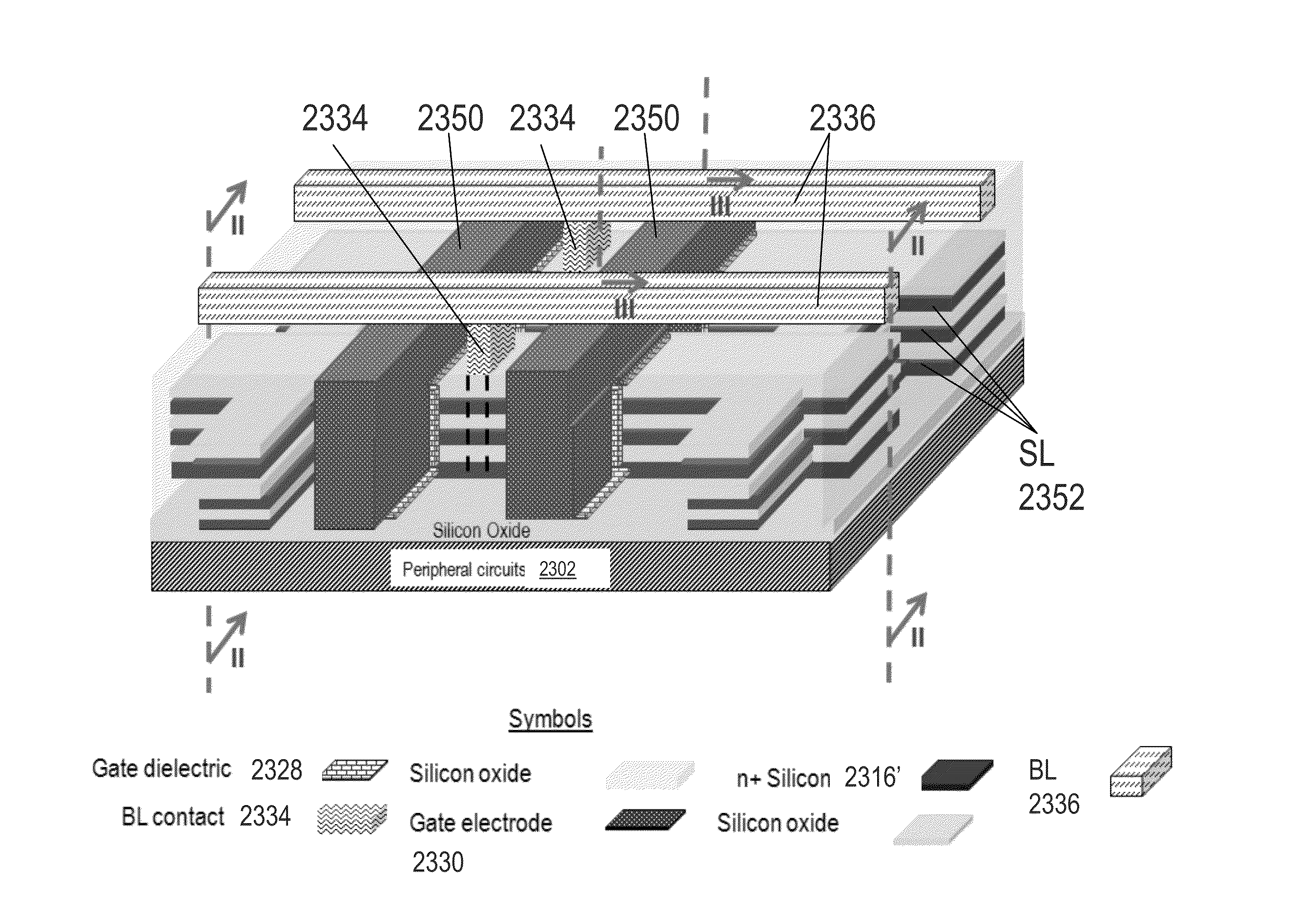
Wherein Wafer Sized Doped Layers are Transferred and then Processed to Create 3D ICs.

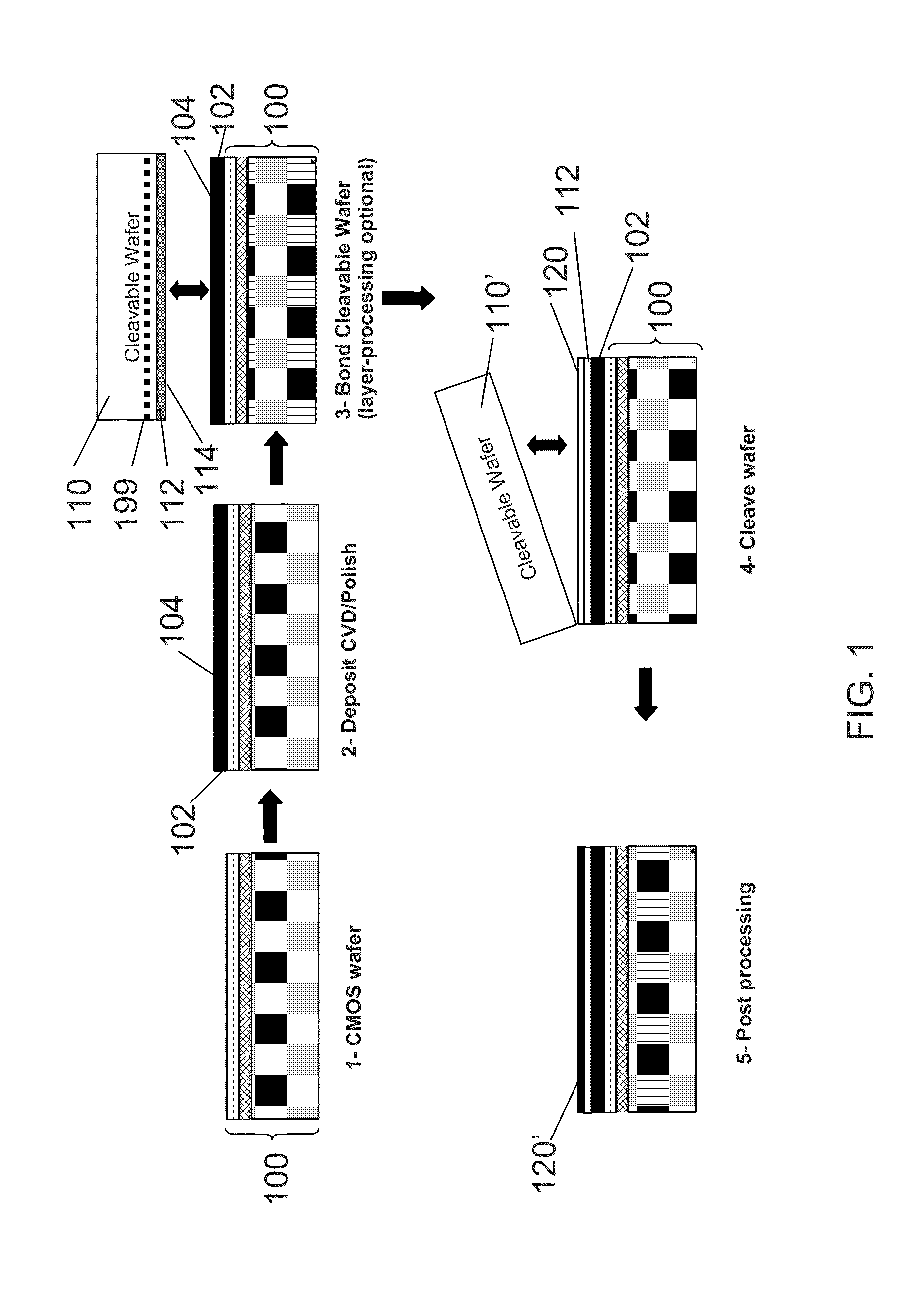
[0113]An embodiment of this invention is to pre-process a donor wafer by forming wafer sized layers of various materials without a process temperature restriction, then layer transferring the pre-processed donor wafer to the acceptor wafer, and processing at either low temperature (below approximately 400° C.) or high temperature (greater than approximately 400° C.) after the layer transfer to form device structures, such as transistors, on or in the donor wafer that may be physically aligned and may be electrically coupled or connected to the acceptor wafer. A wafer sized layer denotes a continuous layer of material or combination of materials that extends across the wafer to the full extent of the wafer edges and may be approximately uniform in thickness. If the wafer sized layer compromises dopants, then the dopant concentration may be substantially the same in the x and y direction across the wa...


PUM


Abstract

A method for fabricating a device, the method including: providing a first layer including first transistors, where the first transistors include a mono-crystalline semiconductor; overlaying a second semiconductor layer over the first layer; fabricating a plurality of memory cell control lines where the control lines include a portion of the second layer; where the second layer includes second transistors, where the second transistors include a mono-crystalline semiconductor, and where the second transistors are configured to be memory cells.

Description

BACKGROUND OF THE INVENTION[0001]1. Field of the Invention[0002]The invention relates to multilayer or Three Dimensional Integrated Circuit (3D IC) devices, structures, and fabrication methods.[0003]2. Discussion of Background Art[0004]Performance enhancements and cost reductions in generations of electronic device technology has generally been achieved by reducing the size of the device, resulting in an enhancement in device speed and a reduction in the area of the device, and hence, its cost. This is generally referred to as ‘device scaling’. The dominant electronic device technology in use today is the Metal-Oxide-Semiconductor field effect transistor (MOSFET) technology.[0005]Performance and cost are driven by transistor scaling and the interconnection, or wiring, between those transistors. As the dimensions of the device elements have approached the nanometer scale, the interconnection wiring now dominates the performance, power, and density of integrated circuit devices as des...

Claims


Application Information

Patent Timeline
Patent Type & Authority Patents(United States)
IPC IPC(8): H01L21/44H01L21/822H01L21/82
CPCH01L2224/16225H01L27/092H01L27/0688H01L23/481H01L27/0623H01L29/785H01L29/0673H01L27/088H01L27/082H01L21/76898H01L2924/16152H01L24/05H01L21/268H01L27/1203H01L21/76254H01L29/66545H01L21/84H01L2924/12032H01L2924/1305H01L2924/1306H01L2924/13062H01L2924/13091H01L2924/15788H01L2924/351H01L2224/0401H01L2924/00
Inventor SEKAR, DEEPAKOR-BACH, ZVICRONQUIST, BRIAN
Owner MONOLITHIC 3D
Why Eureka
Try Eureka