High frequency module

a high-frequency module and module technology, applied in the field of high-frequency modules, can solve the problems of large warpage, adversely affecting the grinding accuracy of the semiconductor substrate, and easy damage of the semiconductor substrate 104/b>, so as to facilitate the grinding process of the first component, improve the shielding performance of the first component and the second component, and reduce the warpage of the semi-finished product after the first sealing resin layer

Active Publication Date: 2021-02-11
MURATA MFG CO LTD
View PDF0 Cites 0 Cited by
  • Summary
  • Abstract
  • Description
  • Claims
  • Application Information

AI Technical Summary

Benefits of technology

[0014]The high frequency module may further include a shield film that coats at least the side surface of the first sealing resin layer, a side surface of the wiring board, and the side surface and the opposing surface of the second sealing resin layer. In this case, the shielding performance for the first component and the second component can be improved.
[0015]According to the present disclosure, because the warpage of the semi-finished product after the first sealing resi

Problems solved by technology

In particular, when the module 100 is manufactured in a collective board, the warpage tends to become large because the area is large.
The warpage of the collective board adversely affects the grinding accuracy of the semiconductor substrate 104.
However, because the linear expansion coefficient o

Method used


Image

  • High frequency module
  • High frequency module
  • High frequency module

Examples


first embodiment

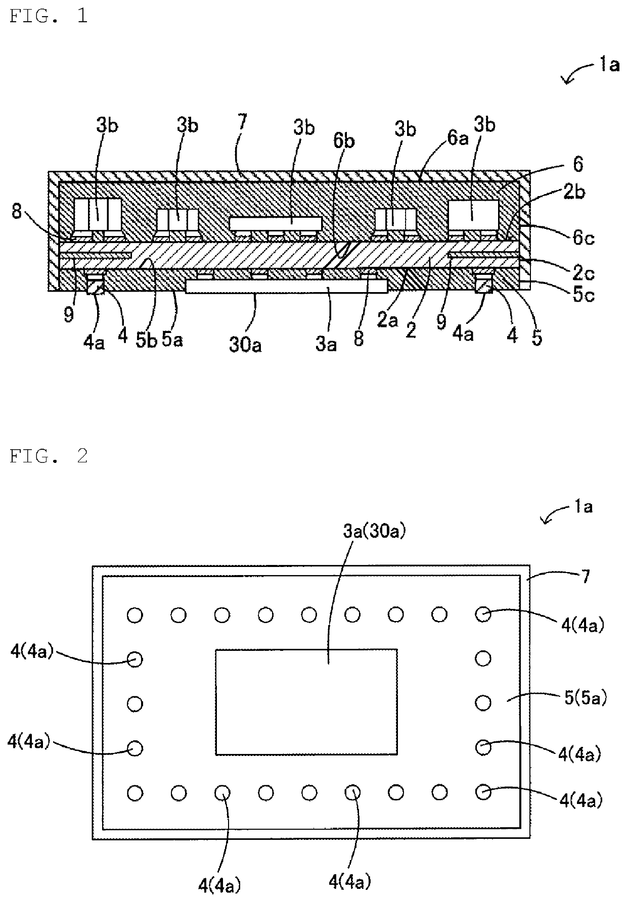
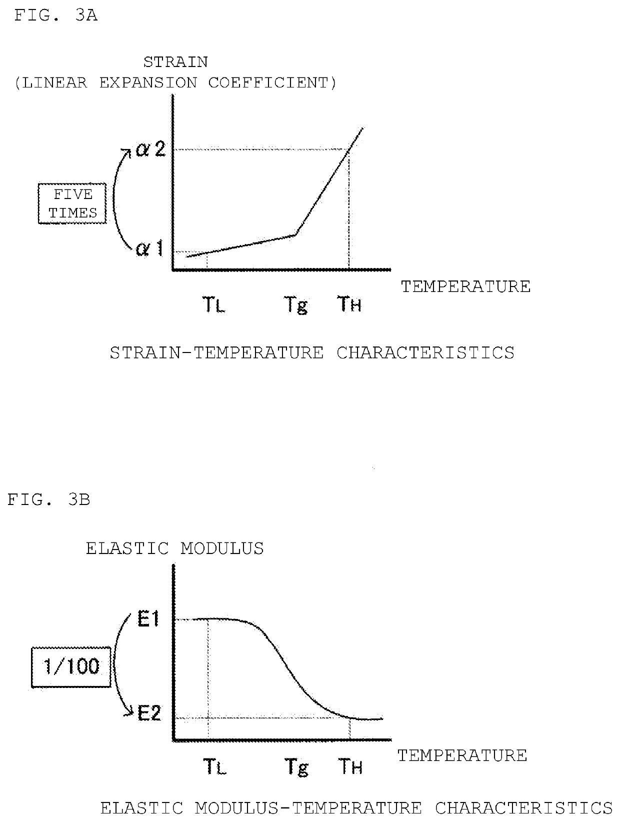
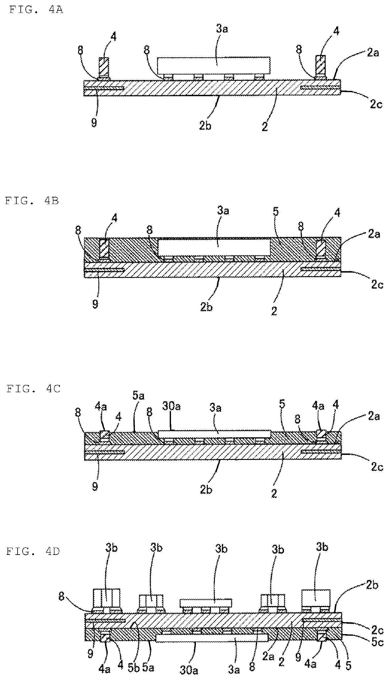
[0026]The configuration of a high frequency module 1a according to a first embodiment of the present disclosure is described with reference to FIGS. 1 to 5C. Note that FIG. 1 is a sectional view of the high frequency module 1a, FIG. 2 is a plan view showing a lower surface 5a of a first sealing resin layer 5 of the high frequency module 1a, FIGS. 3A and 3B are graphs showing relationships between a glass transition temperature, and a linear expansion coefficient and an elastic modulus, and FIGS. 4A to 4D and 5A to 5C are views showing a manufacturing process of the high frequency module 1a.

[0027]As shown in FIGS. 1 and 2, the high frequency module 1a according to this embodiment includes a wiring board 2, a first component 3a and a plurality of connection terminals 4 mounted on a lower surface 2a of the wiring board 2, a first sealing resin layer 5 that seals the first component 3a and the connection terminals 4, a plurality of second components 3b mounted on an upper surface 2b of...

second embodiment

[0047]A high frequency module 1b according to a second embodiment of the present disclosure is described with reference to FIGS. 6 and 7. FIG. 6 is a cross-sectional view of the high frequency module 1b, and FIG. 7 is a plan view showing a lower surface 5a of a first sealing resin layer 5 of the high frequency module 1b.

[0048]The high frequency module 1b according to this embodiment is different from the high frequency module 1a of the first embodiment described with reference to FIGS. 1 and 2 in that, as shown in FIGS. 6 and 7, a plurality of first components 3a are mounted on a lower surface 2a of a wiring board 2 and connection terminals 4 are arranged between the adjacent first components 3a. Other configurations are the same as those of the high frequency module 1a according to the first embodiment, and therefore, the same reference numerals are given and the descriptions thereof are omitted.

[0049]In this embodiment, the two first components 3a are mounted on the lower surface...

third embodiment

[0051]A high frequency module 1c according to a third embodiment of the present disclosure is described with reference to FIGS. 8 and 9. FIG. 8 is a sectional view of the high frequency module 1c, and FIG. 9 is a plan view showing a lower surface 5a of a first sealing resin layer 5 of the high frequency module 1c.

[0052]The high frequency module 1c according to this embodiment is different from the high frequency module 1a of the first embodiment described with reference to FIGS. 1 and 2 in that, as shown in FIGS. 8 and 9, a plurality of connection terminals 40 for external connection are formed as bumps. Other configurations are the same as those of the high frequency module 1a according to the first embodiment, and therefore, the same reference numerals are given and the descriptions thereof are omitted.

[0053]In this embodiment, each of the connection terminals 40 is formed as a bump such as a solder bump or a gold bump on the mounting electrode 8. The connection terminals 40 are ...


PUM


Abstract

A high frequency module in which warpage does not easily occur is provided by adjusting linear expansion coefficient, glass transition temperature, and elastic modulus of a sealing resin layer. The high frequency module includes a wiring board, a first component mounted on a lower surface of the wiring board, a plurality of connection terminals, a first sealing resin layer that coats the first component and the connection terminal, a plurality of second components mounted on an upper surface of the wiring board, a second sealing resin layer coating the second components, and a shield film. The first sealing resin layer is formed thinner than the second sealing resin layer, and the first sealing resin layer has the linear expansion coefficient of the resin smaller than the linear expansion coefficient of the resin of the second sealing resin layer.

Description

CROSS REFERENCE TO RELATED APPLICATIONS[0001]This is a continuation of International Application No. PCT / JP2019 / 018207 filed on May 7, 2019 which claims priority from Japanese Patent Application No. 2018-089657 filed on May 8, 2018. The contents of these applications are incorporated herein by reference in their entireties.BACKGROUND OF THE DISCLOSUREField of the Disclosure[0002]The present disclosure relates to a high frequency module in which components are mounted on one main surface of a wiring board and the components are coated with a sealing resin layer.Description of the Related Art[0003]Conventionally, there is proposed a high frequency module, as in a module 100 shown in FIG. 10, in which a plurality of chip components 102 coated with a second resin layer 103 are mounted on an upper surface 101a of a wiring board 101, and a semiconductor substrate 104 and connection terminals 105 coated with a first resin layer 106 are mounted on a lower surface 101b of the wiring board 10...

Claims


Application Information

Patent Timeline
IPC IPC(8): H01L23/00H01L23/31H01L23/498H01L23/552H01L23/66H01L21/48H01L21/56
CPCH01L23/562H01L24/08H01L23/3128H01L23/49816H01L23/49838H01L23/552H01L2924/3511H01L21/4853H01L21/565H01L2224/16227H01L2924/19106H01L2924/3025H01L23/66H05K9/00H05K3/28H05K3/00H01L2924/181H01L2924/19105H01L2224/97H01L23/3121H01L21/561H01L23/49811H01L2225/06517H01L2225/06572H01L2224/16238H01L2924/00012H01L2224/81
Inventor NOMURA, TADASHIKUSUYAMA, TAKAFUMI
Owner MURATA MFG CO LTD
Why Eureka
Try Eureka