Adhesion device, micro device optical inspection and repairing equipment and optical inspection and repairing method

a technology of optical inspection and repair equipment, applied in semiconductor devices, semiconductor/solid-state device testing/measurement, instruments, etc., can solve problems such as the number of abnormal micro led chips, and achieve the effect of high repair ra

Active Publication Date: 2021-02-18
PLAYNITRIDE DISPLAY CO LTD
View PDF0 Cites 1 Cited by
  • Summary
  • Abstract
  • Description
  • Claims
  • Application Information

AI Technical Summary

Benefits of technology

[0006]The disclosure provides an ad

Problems solved by technology

In recent years, in the case that the manufacturing cost of an organic light emitting diode (OLED) display panel is relatively high, and the lifetime and the reliability of the OLED display panel cannot compete with an existing mainstream display, a micro LED display gradually attracts various scientific and technic

Method used


Image

  • Adhesion device, micro device optical inspection and repairing equipment and optical inspection and repairing method
  • Adhesion device, micro device optical inspection and repairing equipment and optical inspection and repairing method
  • Adhesion device, micro device optical inspection and repairing equipment and optical inspection and repairing method

Examples


third embodiment

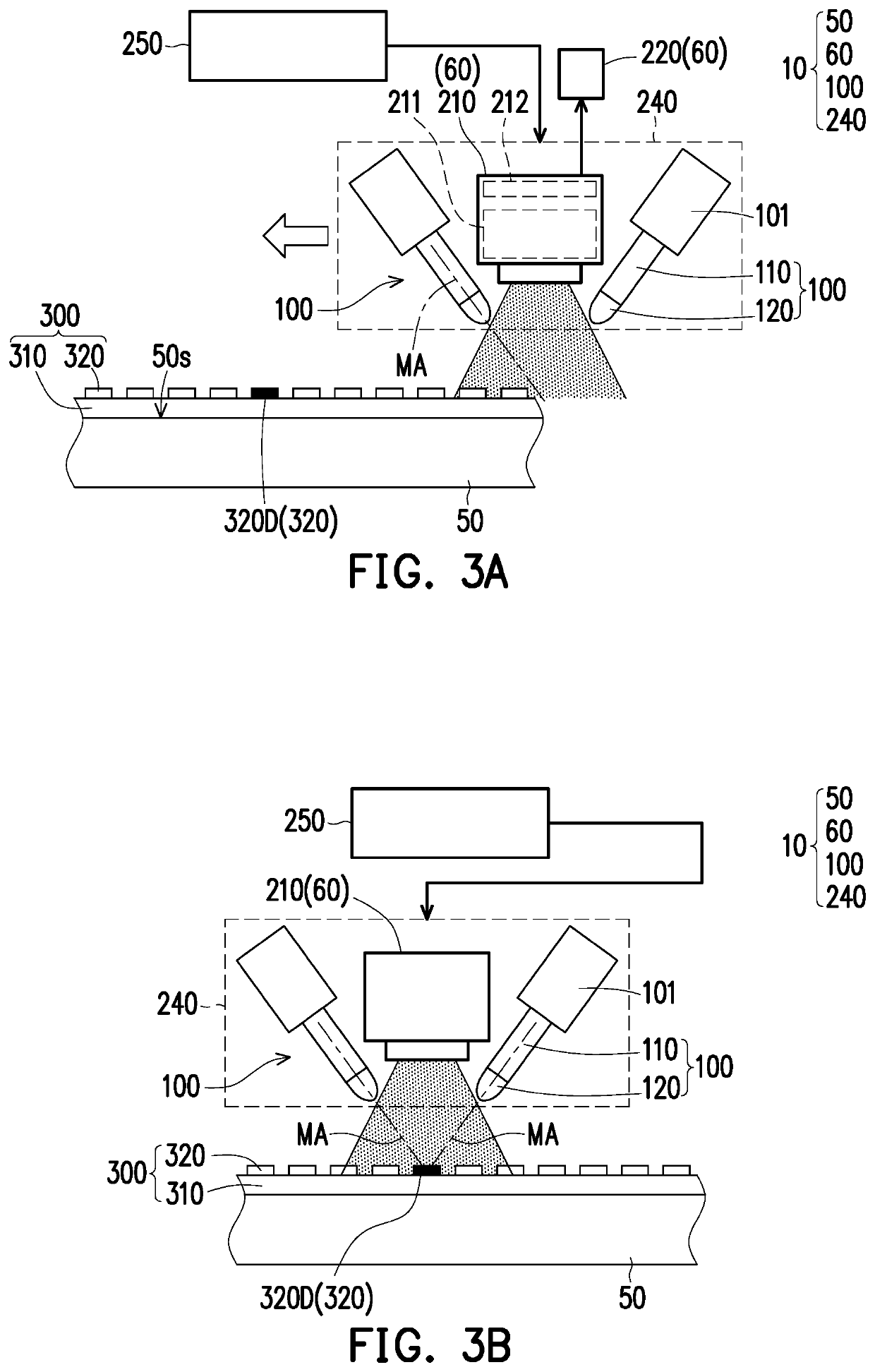
[0059]FIG. 7 is an operation schematic diagram of an adhesion device according to the disclosure. Referring to FIG. 7, a main difference between micro device optical inspection and repairing equipment 12 of the present embodiment and the micro device optical inspection and repairing equipment 11 of FIG. 6 lies in the number and actuation mode of the adhesion devices 100. In the present embodiment, the micro device optical inspection and repairing equipment 12 has multiple adhesion devices 100, and these adhesion devices 100 are disposed on a carrier 101 and arranged in an array.

[0060]For example, in direction D1, any two adjacent micro elements 320 are arranged on the substrate 310 at a first interval P1, and any two adjacent adhesion devices 100 are arranged on the carrier 101 at a second interval P2. In the present embodiment, the second interval P2 is substantially equal to the first interval P1, but the disclosure is not limited thereto. In another embodiment, the second interva...

fourth embodiment

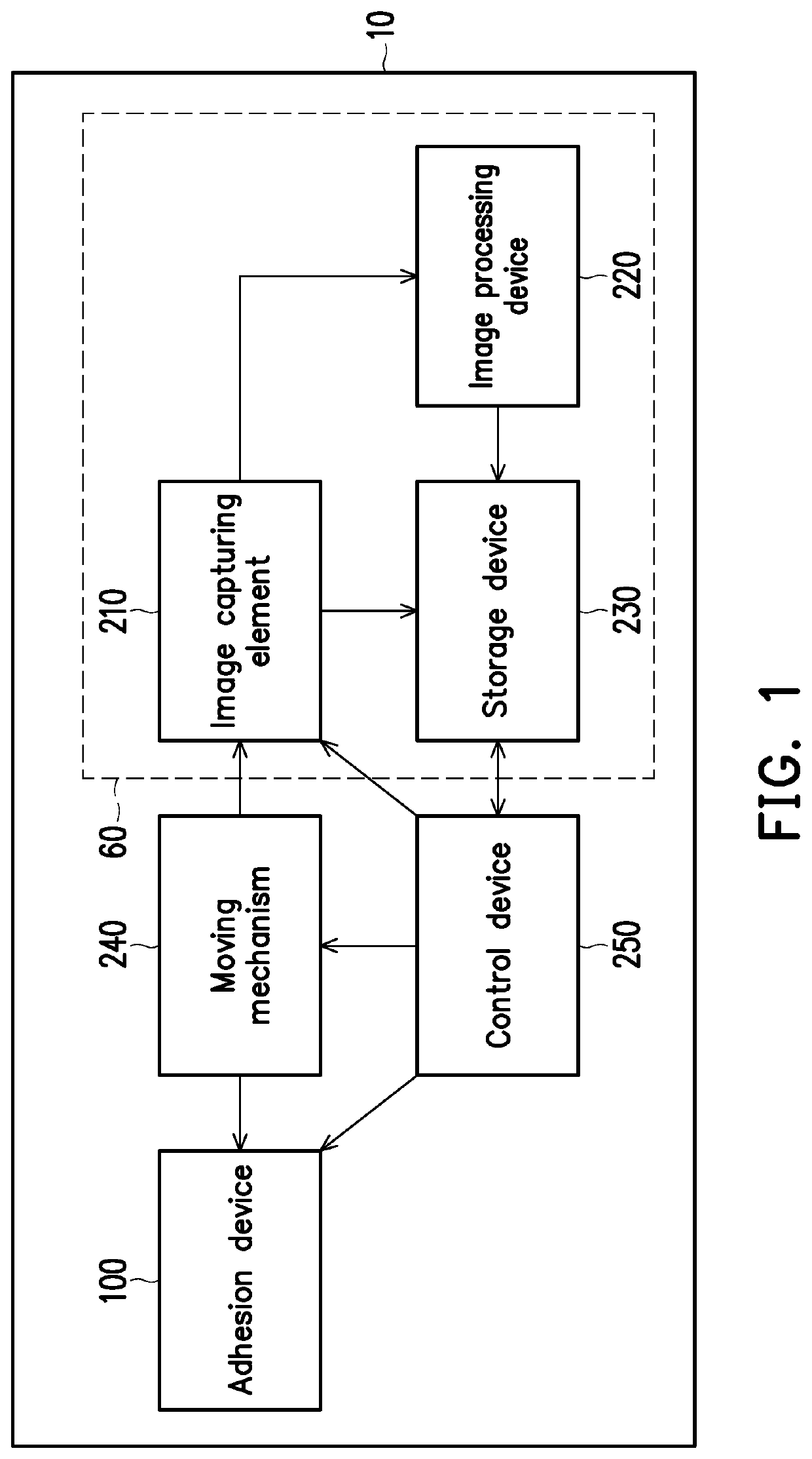
[0061]FIG. 8 is a block diagram of micro device optical inspection and repairing equipment according to the disclosure. Referring to FIG. 8, a main difference between the micro device optical inspection and repairing equipment 13 of the present embodiment and the micro device optical inspection and repairing equipment 11 of FIG. 5 lies in constitutions of the optical inspection modules. In the present embodiment, an optical inspection module 60A may also include a thickness detector 260. The thickness detector 260 here is, for example, a white light interferometer, and may be used to obtain thickness information (such as step height) of micro element of an object under test on a carrying stage. and thickness distribution information (such as film thickness uniformity or surface roughness) of the object under test.

[0062]Based on the above, in the micro device optical inspection and repairing equipment and optical inspection and repairing method of one embodiment of the disclosure, th...


PUM


Abstract

Micro device optical inspection and repairing equipment adopting an adhesion device is provided. The micro device optical inspection and repairing equipment includes a carrying stage, an optical inspection module and at least one adhesion device. The optical inspection module is arranged corresponding to the carrying stage so as to capture image information and obtain a position coordinate from the image information. The adhesion device includes a main body and an adhesive portion. The adhesive portion is connected to the main body. The adhesion device can move to a target position of the carrying stage according to the position coordinate. The main body is adapted to drive the adhesive portion to move to the target position along a moving axis. An optical inspection and repairing method adopting the micro device optical inspection and repairing equipment is also provided.

Description

CROSS-REFERENCE TO RELATED APPLICATION[0001]This application claims the priority benefit of Taiwan application serial no. 108128876, filed on Aug. 14, 2019. The entirety of the above-mentioned patent application is hereby incorporated by reference herein and made a part of this specification.BACKGROUND1. Technical Field[0002]The disclosure generally relates to a flaw inspection and repairing technique, and in particular, to an adhesion device, micro device optical inspection and repairing equipment and an optical inspection and repairing method.2. Description of Related Art[0003]In recent years, in the case that the manufacturing cost of an organic light emitting diode (OLED) display panel is relatively high, and the lifetime and the reliability of the OLED display panel cannot compete with an existing mainstream display, a micro LED display gradually attracts various scientific and technical manufacturers to make an investment. In addition to the advantages of low energy consumptio...

Claims


Application Information

Patent Timeline
IPC IPC(8): H01L21/66H01L21/67
CPCH01L22/22H01L25/0753H01L21/67288H01L21/67011H01L22/20H01L22/12G01B11/00
Inventor LIN, CHENG-CIAN
Owner PLAYNITRIDE DISPLAY CO LTD
Why Eureka
Try Eureka