
Para-phenylenes as buffer and color tuning layers for solar cells

a technology of paraphenylene and color tuning layer, which is applied in the direction of electrical apparatus, organic semiconductor materials, semiconductor devices, etc., can solve the problem of not being optimally used in window glass-based photovoltaics

Active Publication Date: 2021-02-18
UBIQUITOUS ENERGY INC
View PDF0 Cites 1 Cited by
  • Summary
  • Abstract
  • Description
  • Claims
  • Application Information

AI Technical Summary

Benefits of technology

[0004]Transparent organic photovoltaic (OPV) devices that can be integrated onto windows panes are desirable for providing large surface areas to take advantage of solar energy. In contrast to inorganic semiconductors, the optical characteristics of organic and molecular semiconductors result in absorption spectra that are high

Problems solved by technology

However, while a variety of organic and molecular semiconductors exist, many exhibit strong absorp

Method used


Image

  • Para-phenylenes as buffer and color tuning layers for solar cells
  • Para-phenylenes as buffer and color tuning layers for solar cells
  • Para-phenylenes as buffer and color tuning layers for solar cells

Examples


Embodiment Construction

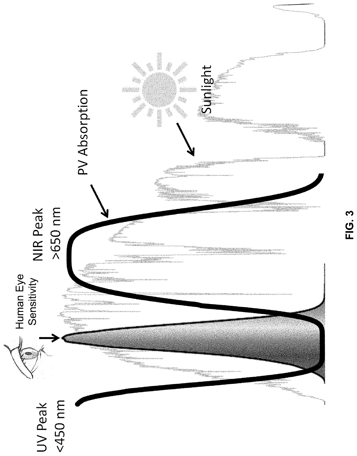
[0077]The present disclosure relates to organic photovoltaic devices (OPVs), and in some embodiments, visibly transparent photovoltaic devices incorporating visibly transparent photoactive compounds. The visibly transparent photoactive compounds absorb light more strongly in the near-infrared and / or ultraviolet regions and less strongly in the visible region, permitting their use in visibly transparent photovoltaic devices. The disclosed visibly transparent photovoltaic devices include visibly transparent electrodes with visibly transparent photoactive materials positioned between the visibly transparent electrodes.

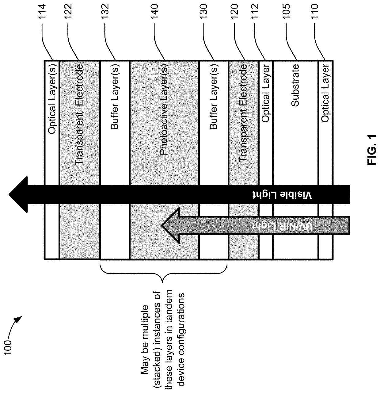
[0078]FIG. 1 illustrates a simplified schematic diagram of a visibly transparent photovoltaic device 100, according to an embodiment of the present invention. As illustrated in FIG. 1, visibly transparent photovoltaic device 100 includes a number of layers and elements discussed more fully below. As discussed herein, visibly transparent indicates that the photovoltaic dev...


PUM


Abstract

Photovoltaic devices having photoactive layers coupled to buffer layers are disclosed. Such devices may be transparent to visible light but absorb near-infrared light and/or ultraviolet light. The photovoltaic devices may include a p-phenylene layer that acts as a buffer layer. The photovoltaic devices may include one or more photoactive layers. The one or more photoactive layers may include a single planar heterojunction, a single bulk heterojunction (BHJ), or multiple stacked BHJs that have complementary absorption characteristics, among other possibilities.

Description

CROSS-REFERENCES TO RELATED APPLICATIONS[0001]This application claims the benefit of priority to U.S. Provisional Patent Application No. 62 / 887,983, filed Aug. 16, 2019, entitled “PARA-PHENYLENES AS BUFFER AND COLOR TUNING LAYERS FOR SOLAR CELLS,” the entire content of which is incorporated herein by reference for all purposes.BACKGROUND OF THE INVENTION[0002]Photovoltaic devices are commonly employed to convert light into electricity by using the photovoltaic effect, in which absorbed light causes the excitation of an electron or other charge carrier to a higher-energy state. The separation of charge carriers of opposite types leads to a voltage that can be utilized by an external circuit. Photovoltaic devices, such as photovoltaic solar cells, can be packaged together to constitute a photovoltaic array of a larger photovoltaic system, such as a solar panel. The use of photovoltaic systems to generate electricity is an important form of renewable energy that continues to become a m...

Claims


Application Information

Patent Timeline
IPC IPC(8): H01L51/42H01L51/00H01L51/44
CPCH01L51/4253H01L2251/30H01L51/448H01L51/0001H10K85/20H10K30/30Y02E10/549H10K85/60H10K30/88H10K71/00H10K2102/00
Inventor BARR, MILES C.PANDEY, RICHALOVE, JOHN A.SYKES, MATTHEW E.
Owner UBIQUITOUS ENERGY INC
Learn More