
Method for Detecting Wafer Backside Defect

a backside defect and wafer technology, applied in the field of manufacturing semiconductor integrated circuits, can solve the problems of increasing increasing the difficulty of detecting the backside defect of wafers, and the inability of existing methods to analyze the height distribution of defects, so as to reduce the troubleshooting time of process tools and improve the product yield

Active Publication Date: 2021-03-04
SHANGHAI HUALI INTEGRATED CIRCUIT CORP
View PDF0 Cites 1 Cited by
  • Summary
  • Abstract
  • Description
  • Claims
  • Application Information

AI Technical Summary

Benefits of technology

The patent is about a method to detect defects on the backside of a wafer. The method involves using an oblique incident light source to collect data from the light signals emitted and scattered by defects on the wafer backside. This data is then compared with pre-collected data from a database of signals formed by transforming emitted and scattered light signals collected from various defects. This allows the formation of a 3D distribution map of the defect, which is useful in analyzing the source of the defect and finding the defect quickly. This reduces the time needed for troubleshooting and improves the yield of the wafer products.

Problems solved by technology

The impact of a wafer backside defect (that is, a defect on a backside of a wafer) on a wafer frontside pattern is becoming increasingly serious.
The detection of the wafer backside defect is getting increasingly significant.
The imprint will cause ring-shaped polysilicon residues to be formed on the wafer backside, that is, the backside of the wafer, affecting the photolithography process on the crystal face and causing defocus.
The existing method cannot analyze the height distribution of defects.

Method used


Image

  • Method for Detecting Wafer Backside Defect
  • Method for Detecting Wafer Backside Defect
  • Method for Detecting Wafer Backside Defect

Examples


Embodiment Construction

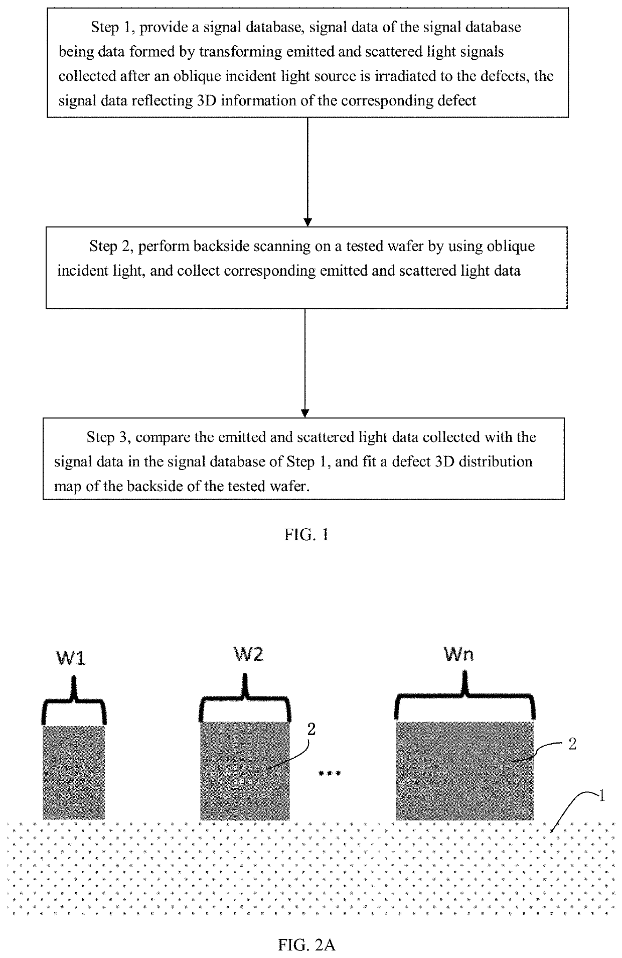
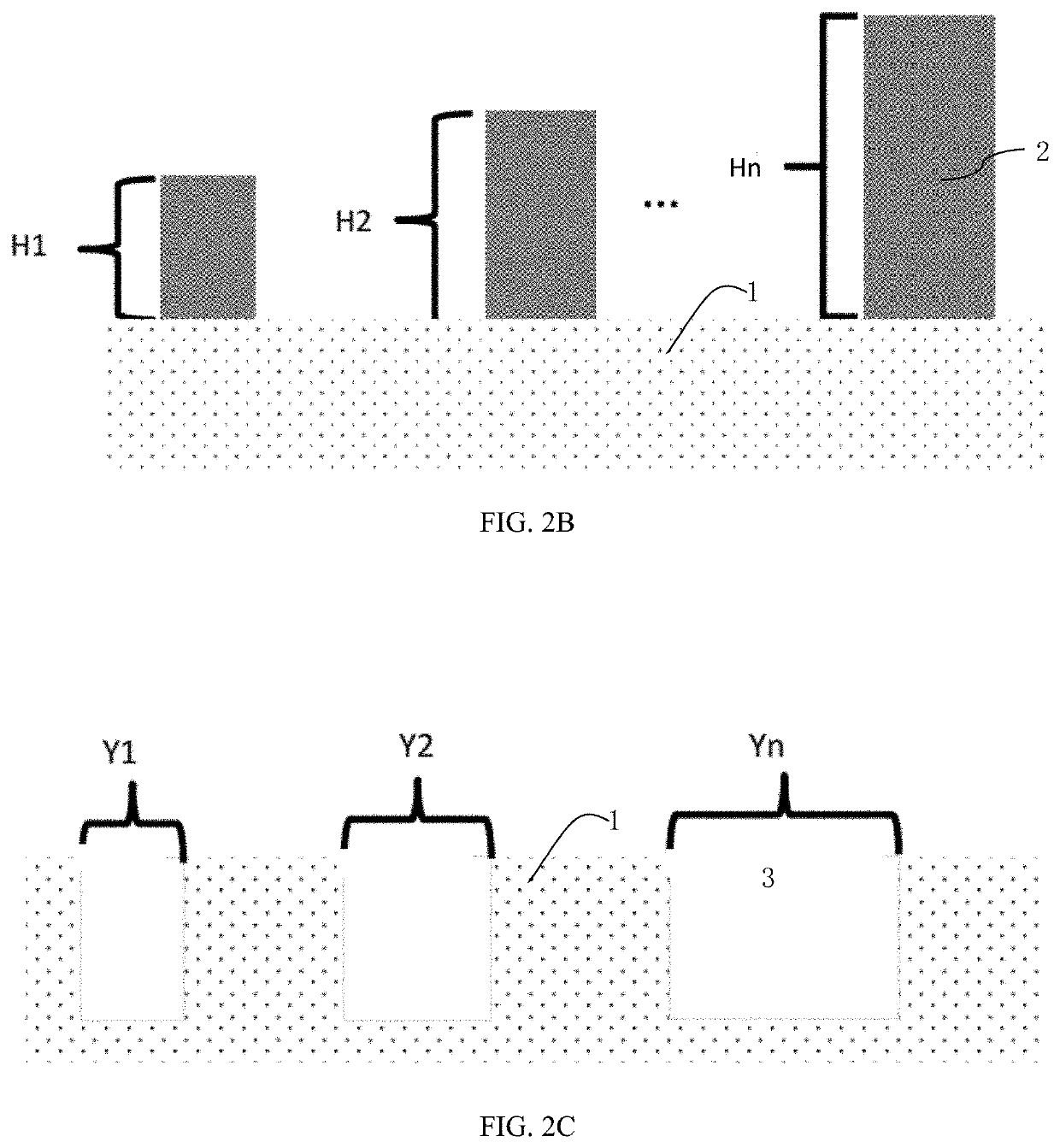
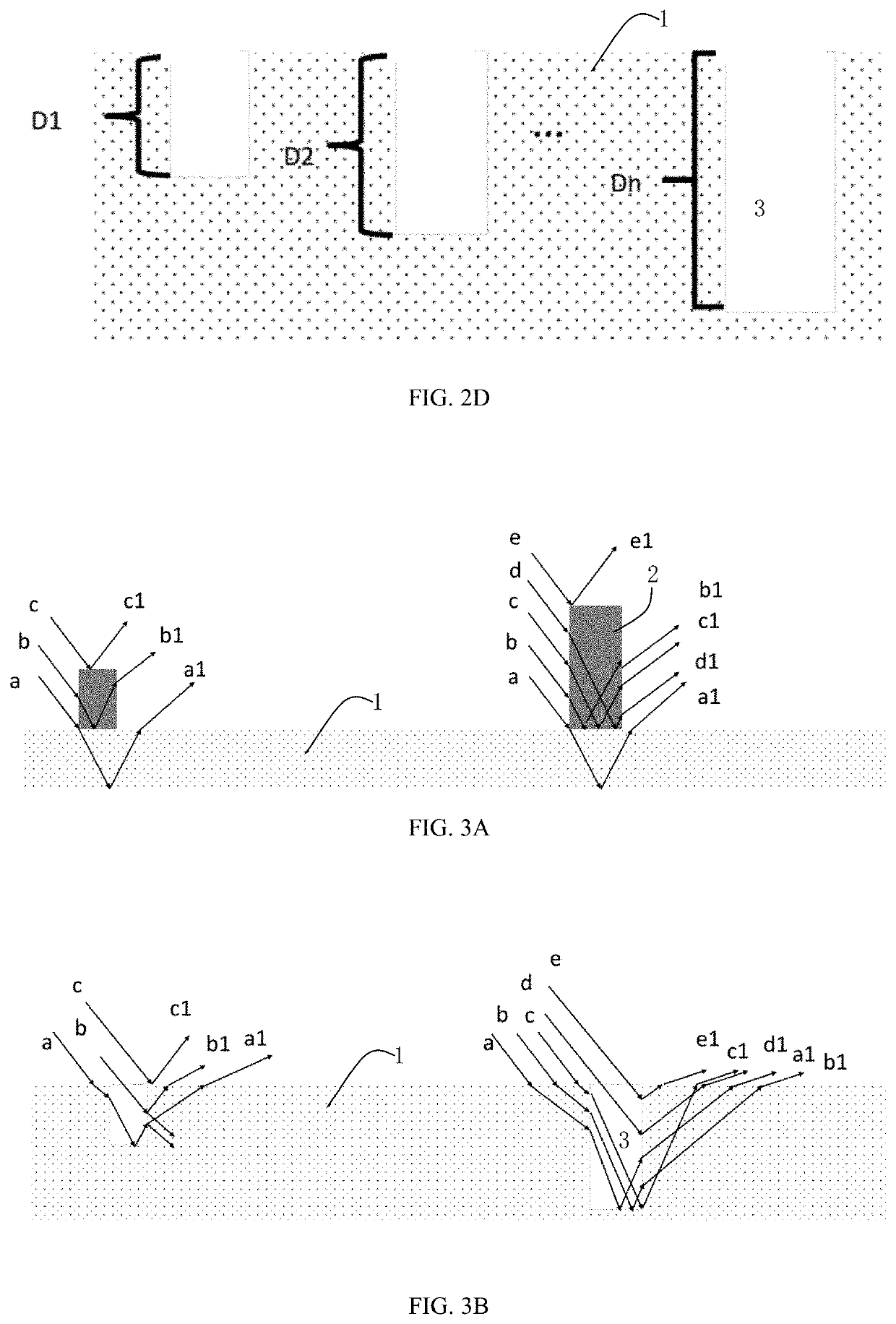
[0047]As shown in FIG. 1, it is a flowchart of a method for detecting a wafer backside defect according to an embodiment of the present disclosure. As shown in FIG. 2A, it is a distribution structure diagram of a first type of test pattern according to an embodiment of the present disclosure. As shown in FIG. 2B, it is a distribution structure diagram of a second type of test pattern according to an embodiment of the present disclosure. As shown in FIG. 2C, it is a distribution structure diagram of a third type of test pattern according to an embodiment of the present disclosure. As shown in FIG. 2D, it is a distribution structure diagram of a fourth type of test pattern according to an embodiment of the present disclosure. The method for detecting a wafer backside defect according to an embodiment of the present disclosure comprises the following steps:

[0048]Step 1, providing a signal database, the signal database comprising signal data corresponding to various different defects, t...


PUM

PropertyMeasurementUnit
defect 3D distributionaaaaaaaaaa
heightaaaaaaaaaa
widthaaaaaaaaaa

Abstract

The present disclosure discloses a method for detecting a wafer backside defect, comprising: Step 1, providing a signal database comprising signal data corresponding to various different defects, the defects comprising convex defects and concave defects, the signal data reflecting 3D information of the corresponding defect; Step 2, performing backside scanning on a tested wafer by using oblique incident light, and collecting corresponding emitted and scattered light data; and Step 3, comparing the collected emitted and scattered light data with the signal data, and fitting a defect 3D distribution map of the backside of the tested wafer. The present disclosure can test the height or depth of a wafer backside defect and form a 3D distribution map of the wafer backside defect, which is beneficial for analyzing the source of the wafer backside defect and processing it in time, reducing the troubleshooting time and improving the product yield.

Description

CROSS REFERENCE TO RELATED APPLICATIONS[0001]The present application claims priority to and the benefit of Chinese Patent Application No. CN 201910809001.3 filed on Aug. 29, 2019, the disclosure of which is incorporated herein by reference in its entirety as part of the present application.TECHNICAL FIELD[0002]The present disclosure relates to a method for manufacturing a semiconductor integrated circuit, in particular to a method for detecting a wafer backside defect.BACKGROUND[0003]In the manufacturing process of semiconductor chips, with the decline of technology nodes, the requirement for forming a device is becoming more and more strict. The impact of a wafer backside defect (that is, a defect on a backside of a wafer) on a wafer frontside pattern is becoming increasingly serious. The detection of the wafer backside defect is getting increasingly significant. The contact part of the process tool in contact with the backside of the wafer will also leave imprints on the wafer bac...

Claims


Application Information

Patent Timeline
Patent Type & Authority Applications(United States)
IPC IPC(8): G01N21/95
CPCG01N21/9505G01N2021/8861H01L22/24H01L22/12G01N2021/887
Inventor YUAN, ZENGYILONG, YINWANG, KAI
Owner SHANGHAI HUALI INTEGRATED CIRCUIT CORP
Learn More