Methods and apparatus for depositing a chalcogenide film and structures including the film

a technology of chalcogenide film and chalcogenide coating, which is applied in the direction of coating, chemical vapor deposition coating, coating process, etc., can solve the problems of difficult production scale up, few, if any, methods for forming electrical contact with semiconducting tmdcs, and difficult production scale up

Pending Publication Date: 2021-03-04
ASM IP HLDG BV
View PDF10 Cites 136 Cited by
  • Summary
  • Abstract
  • Description
  • Claims
  • Application Information

AI Technical Summary

Benefits of technology

[0018]These and other embodiments will become readily apparent from the following detailed description of certain embodi

Problems solved by technology

Furthermore, forming electrical contact to semiconducting TMDCs has turned out to be very difficult using traditional metals with a 3D crystal structure, such as gold and tungsten.
Currently, few, if any, methods are able to deposit uniform films of group 5 dichalcogenides in ultrathin (e.g., less than 10 nm or less than 5 nm) 2D form.
Mechanical exfoliation of bulk crystals has been used for fundamental studies, but such processes are very difficult to scale up for production.
Unfortunately, deposition of films using MBE uses very expensive UHV equipment.
However, CVD usually requires high temperatures of about 600° C. to a

Method used


Image

  • Methods and apparatus for depositing a chalcogenide film and structures including the film
  • Methods and apparatus for depositing a chalcogenide film and structures including the film
  • Methods and apparatus for depositing a chalcogenide film and structures including the film

Examples


Embodiment Construction

[0024]Although certain embodiments and examples are disclosed below, it will be understood by those in the art that the invention extends beyond the specifically disclosed embodiments and / or uses of the invention and obvious modifications and equivalents thereof. Thus, it is intended that the scope of the invention disclosed should not be limited by the particular disclosed embodiments described below.

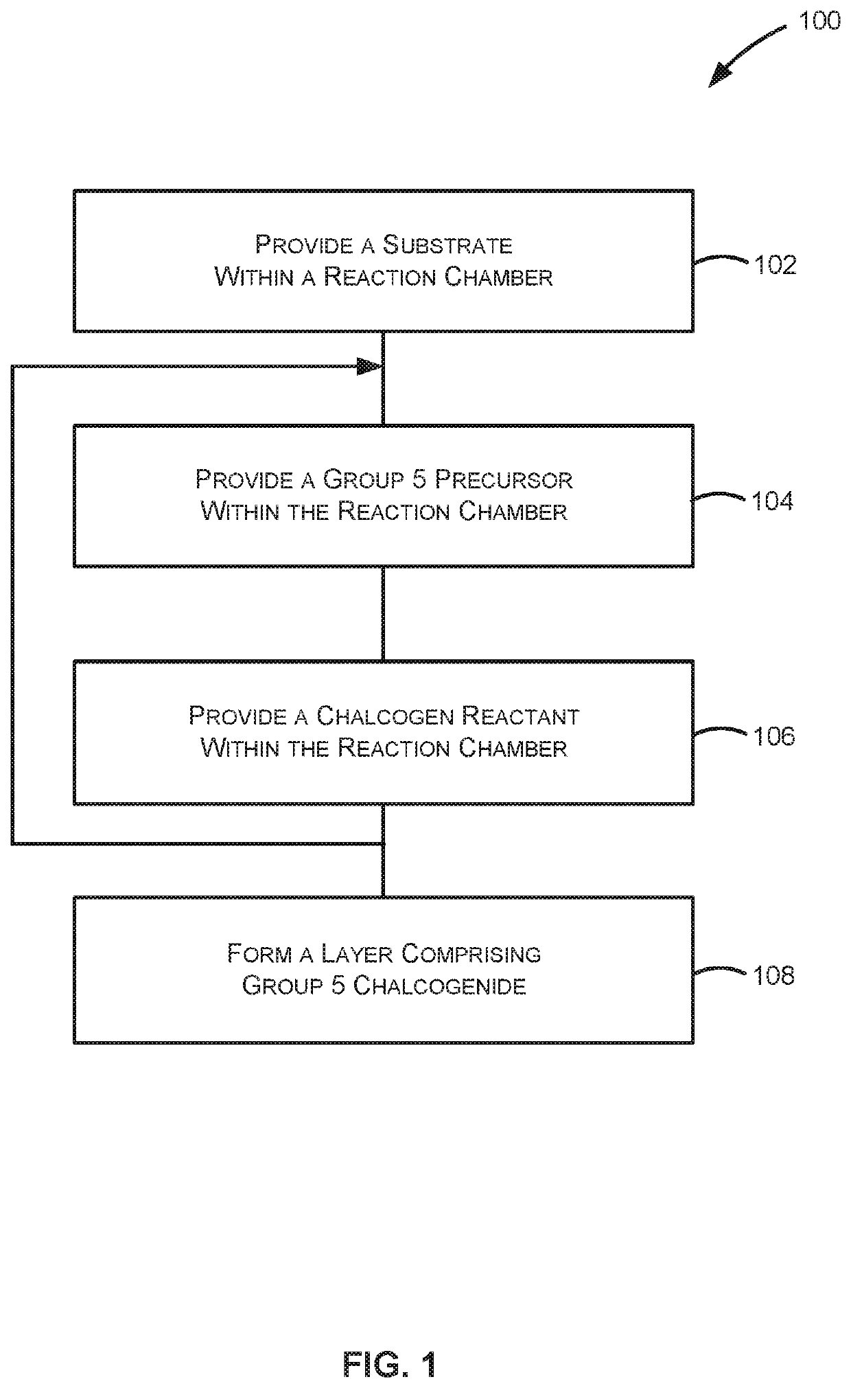
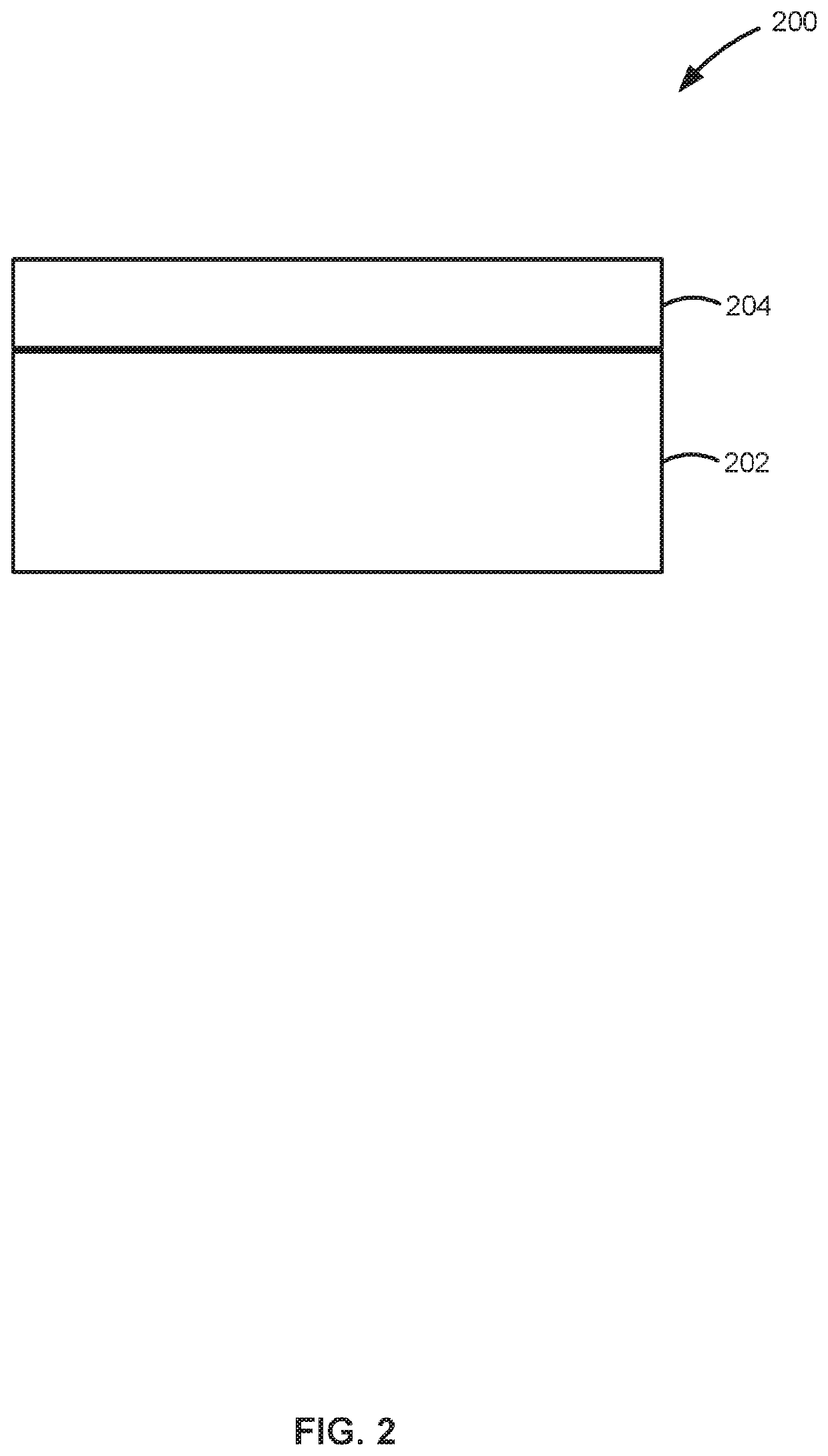
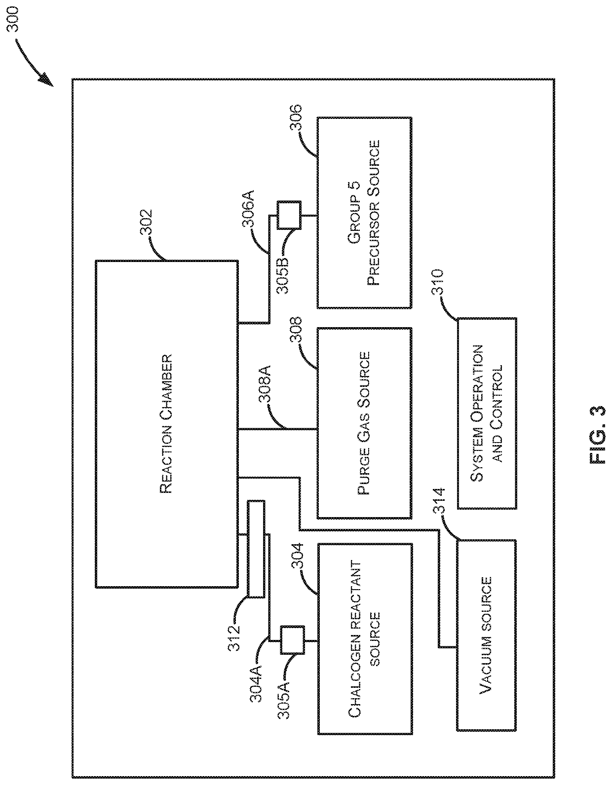
[0025]The present disclosure generally relates to methods of forming structures that include a layer comprising a group 5 chalcogenide, to structures formed using the methods, and to systems for performing the methods and / or forming the structures. Exemplary methods described herein can be used to form structures that include a dichalcogenide, a 2D group 5 chalcogenide and / or a metallic group 5 chalcogenide on the substrate. The structures can be used to form a variety of devices, such as a semiconductor device (e.g., as a contact layer to a semiconductor layer), a supercapacitor, a (e...


PUM

PropertyMeasurementUnit
Temperatureaaaaaaaaaa

Abstract

Methods for depositing group 5 chalcogenides on a substrate are disclosed. The methods include cyclical deposition techniques, such as atomic layer deposition. The group 5 chalcogenides can be two-dimensional films having desirable electrical properties.

Description

CROSS-REFERENCE TO RELATED APPLICATIONS[0001]This application claims priority to U.S. Provisional Patent Application Ser. No. 62 / 895,453 filed Sep. 3, 2019 titled “METHODS AND APPARATUS FOR DEPOSITING A CHALCOGENIDE FILM AND STRUCTURES INCLUDING THE FILM,” the disclosure of which is hereby incorporated by reference in its entirety.PARTIES OF JOINT RESEARCH AGREEMENT[0002]The invention claimed herein was made by, or on behalf of, and / or in connection with a joint research agreement between the University of Helsinki and ASM Microchemistry Oy. The agreement was in effect on and before the date the claimed invention was made, and the claimed invention was made as a result of activities undertaken within the scope of the agreement.FIELD OF INVENTION[0003]The present disclosure relates generally to methods and systems for depositing a chalcogenide film on a substrate. The disclosure also relates to structures including a chalcogenide film.BACKGROUND OF THE DISCLOSURE[0004]Group 5 and oth...

Claims


Application Information

Patent Timeline
IPC IPC(8): H01L21/02C23C16/455C23C16/56C23C16/30
CPCH01L21/02568H01L21/0262C23C16/305C23C16/56C23C16/45553C23C16/45525H01L21/02664C23C16/45536
Inventor MATTINEN, MIIKARITALA, MIKKOLESKELÄ, MARKKU
Owner ASM IP HLDG BV
Why Eureka
Try Eureka