Method and Apparatus for Coupling a Waveguide Structure to an Integrated Circuit Package
a waveguide structure and integrated circuit technology, applied in waveguides, linear waveguide fed arrays, instruments, etc., can solve the problems of generating sufficient power to transmit and providing the required sensitivity to detect signals of millmeter-wave (mmwave or w-band) systems, and consuming significant area on circuit boards
- Summary
- Abstract
- Description
- Claims
- Application Information
AI Technical Summary
Problems solved by technology
Method used
Image

Examples
Embodiment Construction
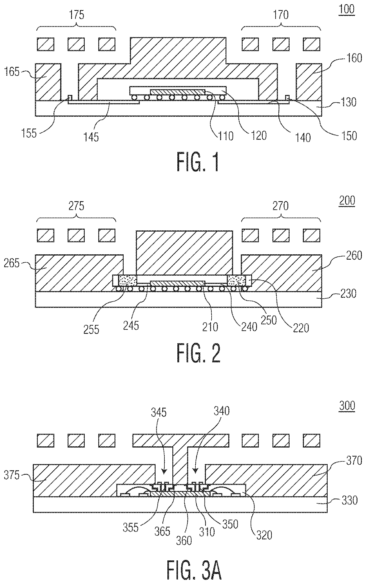
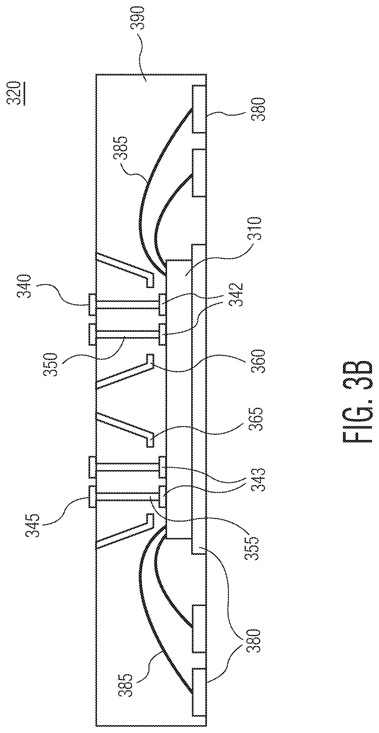
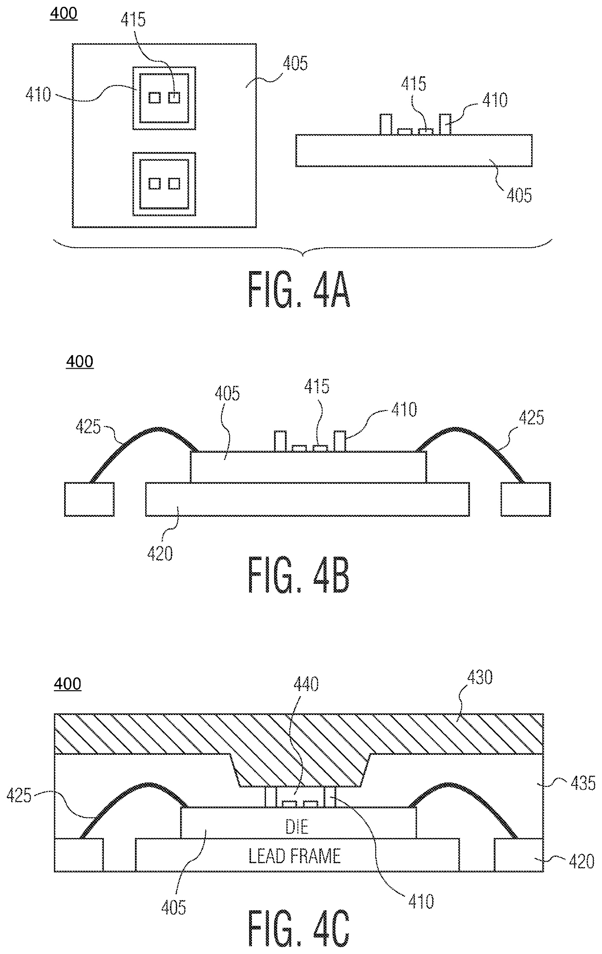
[0015]Embodiments of the present invention are configured to reduce a distance of a waveguide antenna from transmit and receive circuitry in an integrated circuit (IC) device die. Embodiments provide this reduction by providing vertical access to radio frequency (RF) connections on a top surface of the IC device die. A cavity in the encapsulant of the package can be formed to provide access to the connections and plated to perform a shielding function. A continuous connection from the RF pads is used as a vertical interconnect. The region around the vertical interconnect can be filled with encapsulant potting material and back grinded to form a surface of the semiconductor device package. A waveguide antenna feed (e.g., an antenna launcher) can be plated or printed on the vertical interconnect on the surface of the package. Such a mmWave package can be produced in a variety of package type, including, for example, a multi-row quad-flat no-leads (QFN) in a strip or ball grid array pa...
PUM
 Abstract
Description
Claims
Application Information
 - R&D Engineer
- R&D Manager
- IP Professional
- Industry Leading Data Capabilities
- Powerful AI technology
- Patent DNA Extraction
Browse by: Latest US Patents, China's latest patents, Technical Efficacy Thesaurus, Application Domain, Technology Topic.
© 2024 PatSnap. All rights reserved.Legal|Privacy policy|Modern Slavery Act Transparency Statement|Sitemap