

Display device and array substrate thereof
- Summary
- Abstract
- Description
- Claims
- Application Information
AI Technical Summary
Benefits of technology
Problems solved by technology
Method used
Image

Examples
Embodiment Construction
[0019]The following descriptions for the respective embodiments are specific embodiments capable of being implemented for illustrations of the present invention with referring to appended figures.
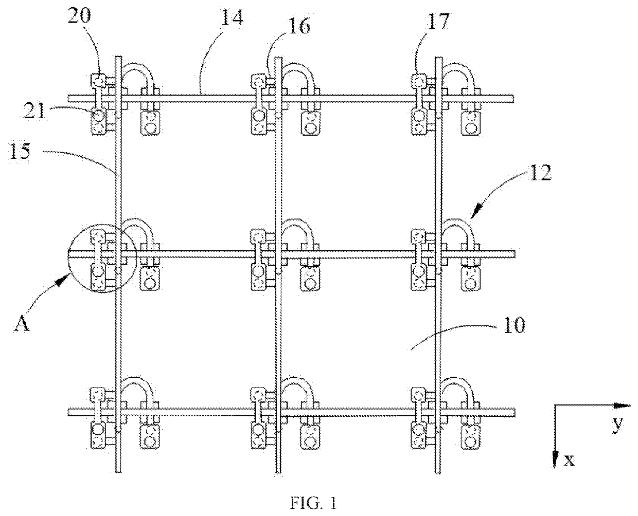
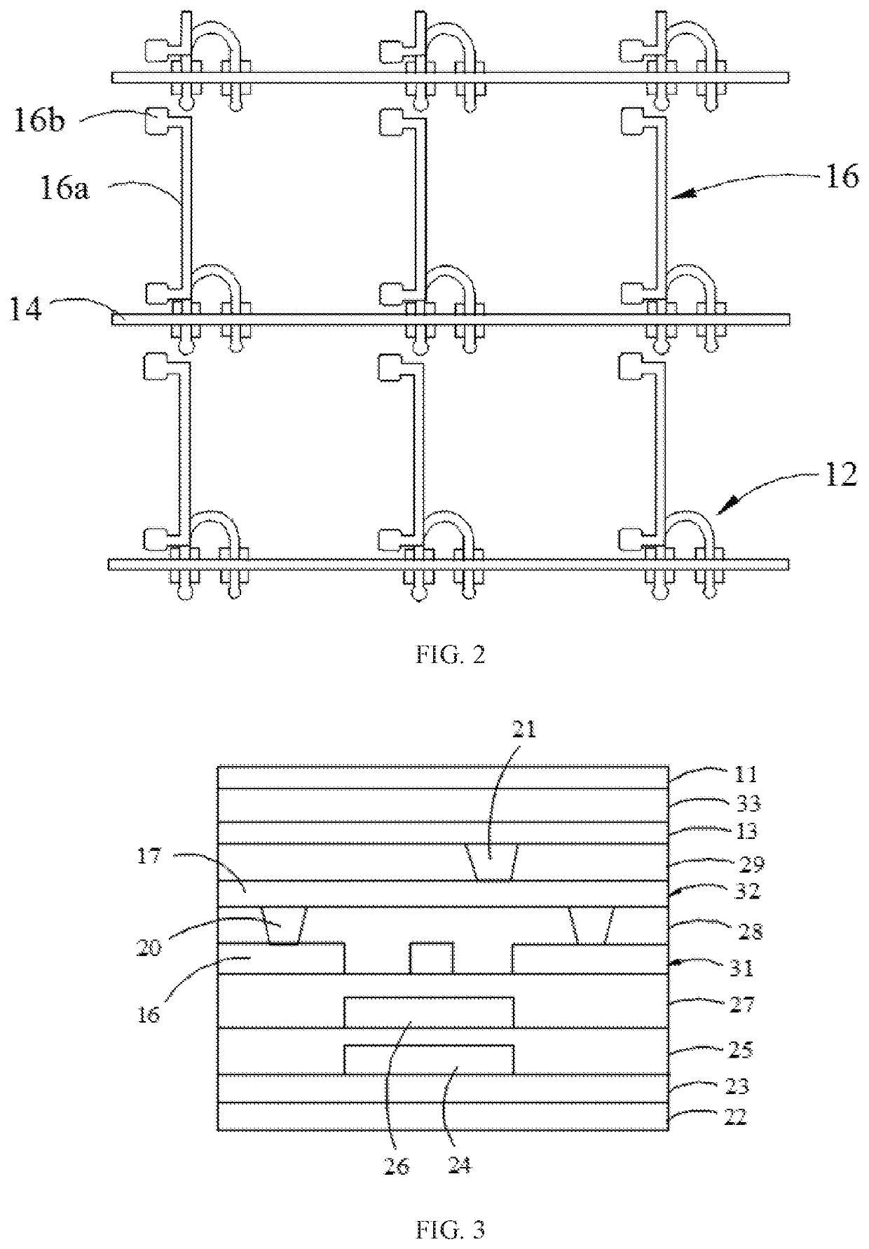
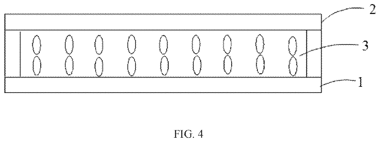
[0020]Please referring to FIGS. 1 to 3. FIG. 1 is a structural schematic diagram of an array substrate according to an embodiment of the present invention but omitting non-conducting film layer, pixel electrodes, and touch electrodes. FIG. 2 is a structural schematic diagram of the array substrate of FIG. 1 without second metallic layer. FIG. 3 is a sectional diagram showing a section of the A area of FIG. 1 along a first direction.
[0021]An array substrate 1 according to an embodiment of the present invention includes multiple pixel units 10 arranged in an array, each including a pixel electrode 11 (see FIG. 3), a thin film transistor (TFT) 12, a touch electrode 13 (see FIG. 3), a scan line 14, and a data line 15. The scan line 14 is configured along a first direction and the data line is c...
PUM
 Abstract
Description
Claims
Application Information