
Method of forming a photoresist underlayer and structure including same

a technology of photoresistance and underlayer, applied in the direction of photomechanical equipment, electrical equipment, basic electric elements, etc., can solve the problems of inability to deposit sog at a thickness of less than 10 nm, the thickness of the substrate-to-substrat, and the inability to meet the thickness of the substrate. , to achieve the effect of reducing the number of lines, reducing the difficulty of forming a structur

Pending Publication Date: 2021-04-15
ASM IP HLDG BV
View PDF6 Cites 133 Cited by
  • Summary
  • Abstract
  • Description
  • Claims
  • Application Information

AI Technical Summary

Benefits of technology

The present patent relates to structures that include a photoresist underlayer, which can improve the performance of photoresist in various ways. The present methods allow for the formation of a relatively thin, uniform photoresist underlayer with desired properties, such as desired etch selectivity, pattern quality, and stability. The photoresist underlayer can be formed using a cyclical process, such as atomic layer deposition, which allows for precise control of the thickness of the photoresist underlayer on a surface of a substrate. The photoresist underlayer can include metal, such as a transition metal, and can be selected and formulated to have desired properties, such as desired surface energy properties. The patent also discusses various precursors, process conditions, treatments, and coatings that can be used to obtain the desired properties of the photoresist underlayer. Overall, the present patent provides improved structures and methods for forming photoresist underlayers with desired properties.

Problems solved by technology

Unfortunately, it can be difficult to deposit SOG at a thickness of less than 10 nm.
Further, a within substrate and substrate-to-substrate thickness non-uniformity of deposited SOG can be undesirably high, particularly as a target thickness of the SOC layer is reduced.
Another challenge encountered when attempting to increase the resolution of lithographical patterning techniques, especially techniques employing EUV photoresist, is related to the EUV photoresist profile after the resist is exposed and developed.
In case the width of the resist lines at the bottom of the structure is lower than the width of the lines at the top of the structures, lines may collapse.
In case the trend is the opposite—lines are wider at the bottom than at the top—lines will be very stable on the underlaying surface, but the pattern transfer will be difficult, and it would result in higher line edge roughness / line width roughness values.
Another challenge encountered when attempting to increase the resolution of lithographical patterning techniques, especially techniques involving EUV photoresist, is related to induced porosity in underlaying layers, e.g. carbon hardmasks, when exposed to depositions and / or surface treatments involving the use of a plasma.

Method used


Image

  • Method of forming a photoresist underlayer and structure including same
  • Method of forming a photoresist underlayer and structure including same
  • Method of forming a photoresist underlayer and structure including same

Examples


Embodiment Construction

[0107]Although certain embodiments and examples are disclosed below, it will be understood that the invention extends beyond the specifically disclosed embodiments and / or uses thereof and obvious modifications and equivalents thereof. Thus, it is intended that the scope of the invention disclosed should not be limited by the particular disclosed embodiments described below.

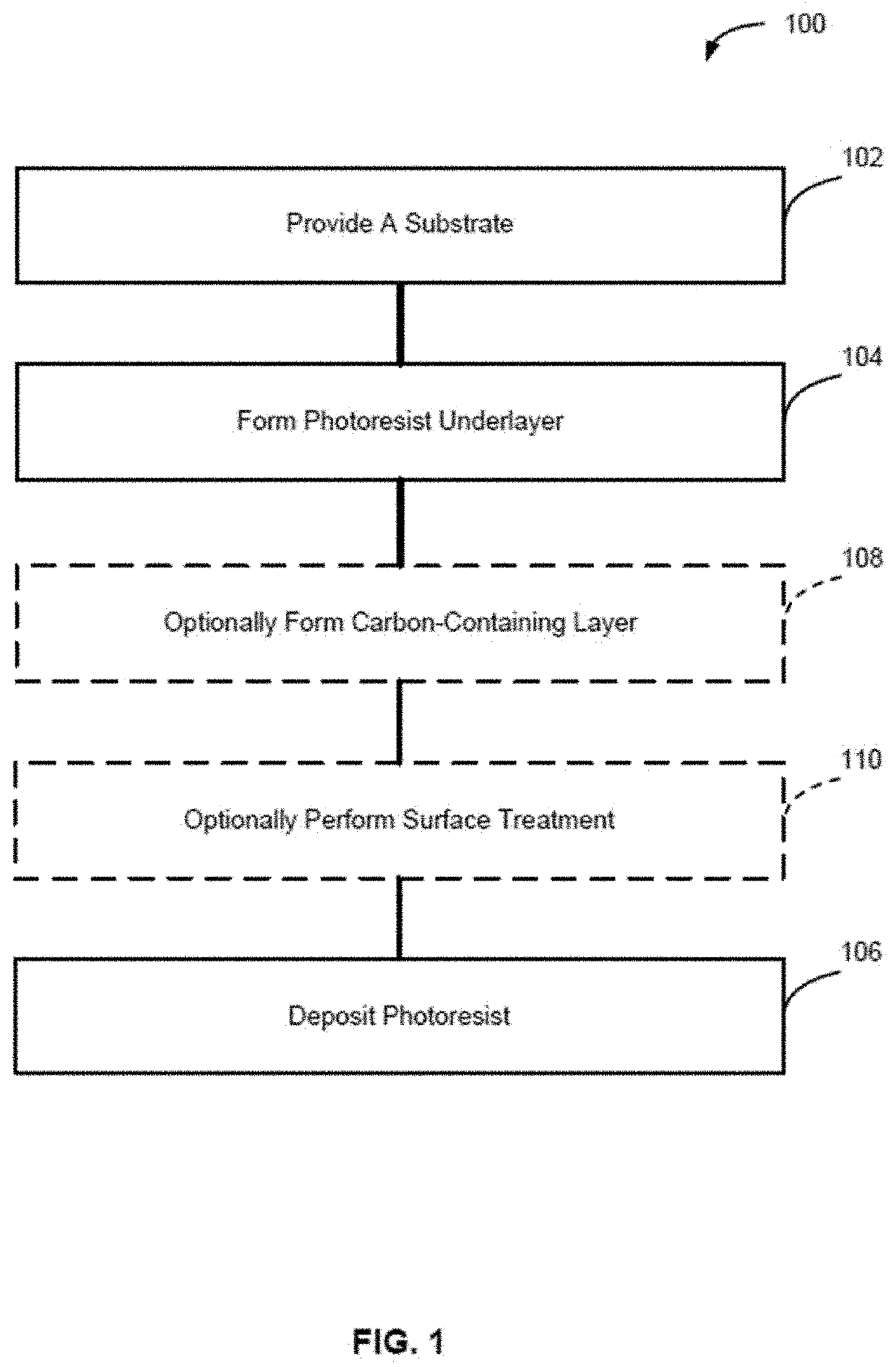
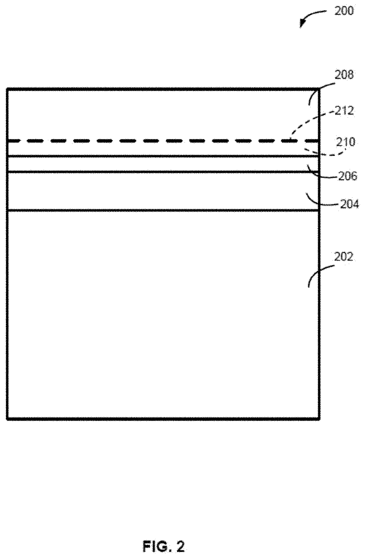
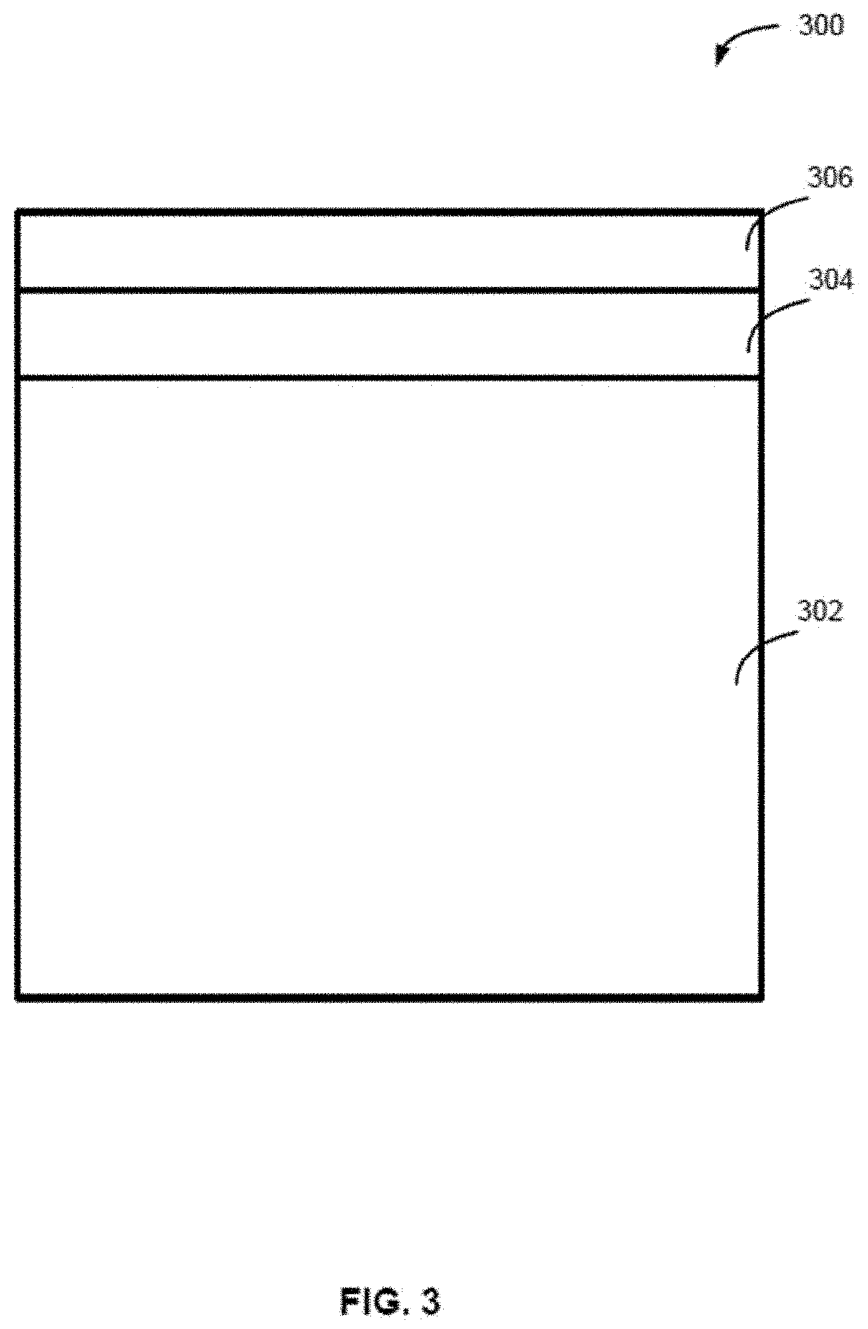
[0108]The present disclosure generally relates to methods of forming structures that include a photoresist underlayer and to structures including a photoresist underlayer. As described in more detail below, exemplary methods can be used to form structures with photoresist underlayers that provide desired properties, such as desired thickness (e.g., less than 10 or less than 5 nm), relatively low surface roughness, good adhesion to the photoresist, desired etch selectivity, desired thickness uniformity—both within a substrate (e.g., a wafer) and between substrates, high pattern quality (low number of defects and hi...


PUM


Abstract

Methods of forming structures including a photoresist underlayer and structures including the photoresist underlayer are disclosed. Exemplary methods include forming the photoresist underlayer that includes metal. Techniques for treating a surface of the photoresist underlayer and / or depositing an additional layer overlying the photoresist underlayer are also disclosed.

Description

CROSS-REFERENCE TO RELATED APPLICATIONS[0001]This application claims priority to U.S. Provisional Patent Application Ser. No. 62 / 913,262 filed Oct. 10, 2019, titled “METHOD OF FORMING A PHOTORESIST UNDERLAYER AND STRUCTURE INCLUDING SAME,” and U.S. Provisional Patent Application Ser. No. 63 / 060,777 filed Aug. 4, 2020, titled METHOD OF FORMING A PHOTORESIST UNDERLAYER AND STRUCTURE INCLUDING SAME, the disclosures of which are hereby incorporated by reference in their entirety.FIELD OF INVENTION[0002]The present disclosure generally relates to structures and to methods of forming structures. More particularly, the disclosure relates to structures including or formed using a photoresist underlayer and to methods of forming such structures.BACKGROUND OF THE DISCLOSURE[0003]During the manufacture of electronic devices, fine patterns of features can be formed on a surface of a substrate by patterning the surface of the substrate and etching material from the substrate surface using, for e...

Claims


Application Information

Patent Timeline
IPC IPC(8): H01L21/033H01L21/027
CPCH01L21/0337H01L21/0332H01L21/0273H01L21/0228H01L21/02186H01L21/02274H01L21/3105H01L21/022G03F7/11H01L21/02172H01L21/02205
Inventor ZYULKOV, IVANDE ROEST, DAVID KURTTOMCZAK, YOANNGIVENS, MICHAEL EUGENESIPPOLA, PERTTUIVANOVA, TATIANALIU, ZECHENGKIM, BOKHEONPIUMI, DANIELE
Owner ASM IP HLDG BV
Features
  • Generate Ideas
  • Intellectual Property
  • Life Sciences
  • Materials
  • Tech Scout
  • Unparalleled Data Quality
  • Higher Quality Content
  • 60% Fewer Hallucinations
Learn More