
Nonvolatile memory device.

a memory device and non-volatile technology, applied in the field of semiconductor memory, can solve the problems of deformation, low conductivity materials, etc., and achieve the effect of preventing a reduction of performance and reducing conductivity

Active Publication Date: 2021-04-22
SAMSUNG ELECTRONICS CO LTD
View PDF0 Cites 3 Cited by
  • Summary
  • Abstract
  • Description
  • Claims
  • Application Information

AI Technical Summary

Benefits of technology

The patent text describes a way to make a memory device that doesn't have any layers with low conductivity. This helps to improve performance while using these layers.

Problems solved by technology

Due to various process issues, some of the conductive layers of the nonvolatile memory device may include a material having lower conductivity than the remaining conductive layers.
However, such lower conductivity materials tend to degrade performance.

Method used


Image

  • Nonvolatile memory device.
  • Nonvolatile memory device.
  • Nonvolatile memory device.

Examples


Embodiment Construction

[0025]Below, various exemplary embodiments will be described in detail and clearly to such an extent that an ordinary one in the art may easily implements the inventive concepts of the present disclosure.

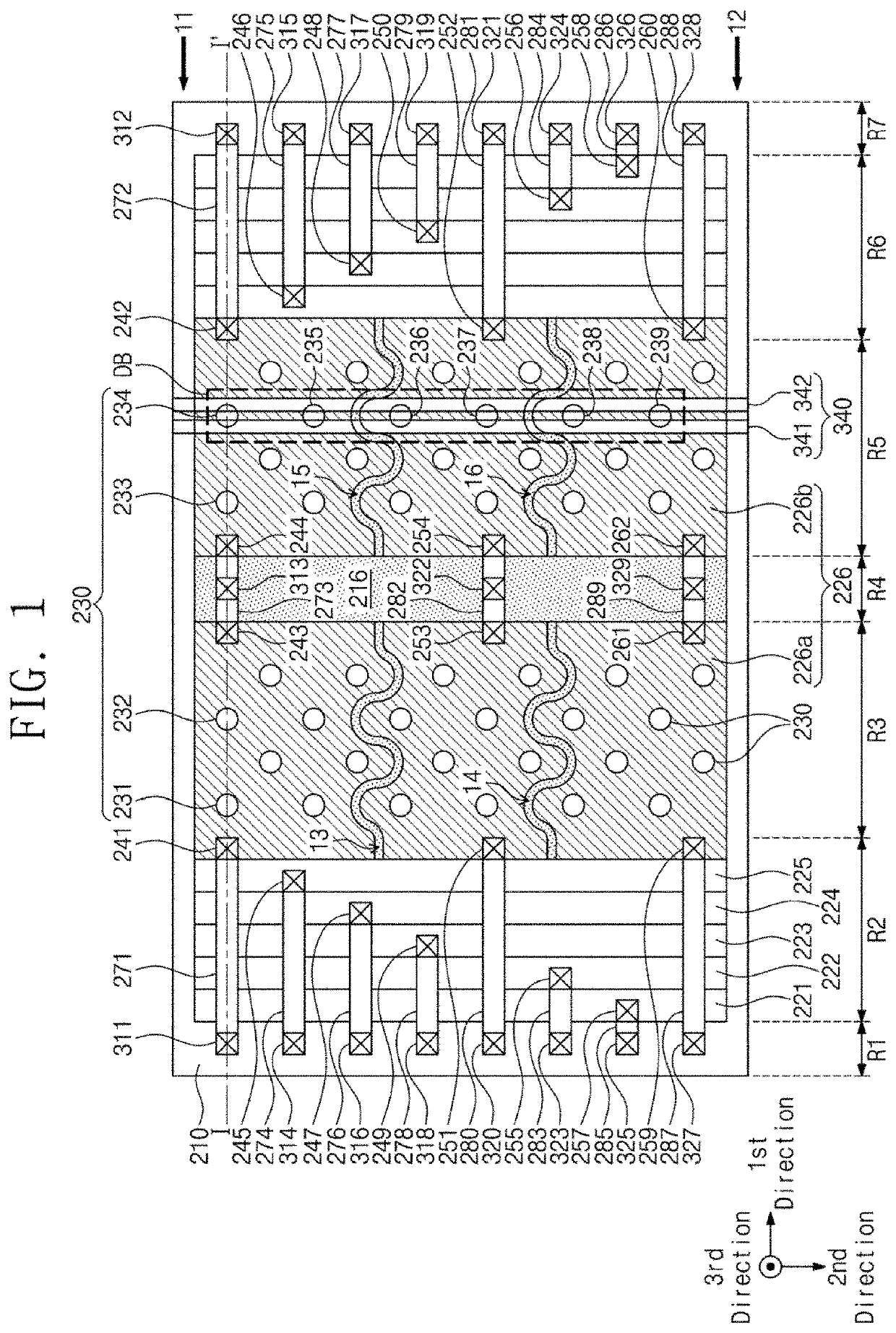
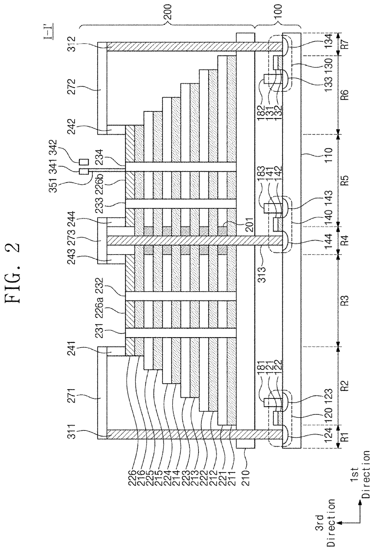
[0026]FIG. 1 is a plan view illustrating a nonvolatile memory device according to an exemplary embodiment. FIG. 2 is a cross-sectional view of the nonvolatile memory device taken along a line I-I′ of FIG. 1.

[0027]Referring to FIGS. 1 and 2, a nonvolatile memory device may include a peripheral circuit 100 and a memory block 200 on the peripheral circuit 100. For example, the nonvolatile memory device may include a cell over peri (COP) structure.

[0028]The peripheral circuit 100 may include a first active region 110, and a plurality of elements 120, 130, and 140 on the first active region 110. The first active region 110 may be formed on a semiconductor substrate. The elements 120, 130, and 140 may include a first pass transistor 120, a second pass transistor 130, and a third pass tran...


PUM

PropertyMeasurementUnit
conductiveaaaaaaaaaa
threshold distanceaaaaaaaaaa
voltageaaaaaaaaaa

Abstract

A nonvolatile memory device includes a memory cell region including first metal pads, and a peripheral circuit region including second metal pads. The memory cell region includes a vertical structure including pairs of a first insulating layer and a first conductive layer, a second insulating layer on the vertical structure, a second conductive layer and a third conductive layer spaced apart from each other on the second insulating layer, first vertical channels and second vertical channels. The second conductive layer and the third conductive layer are connected with a first through via penetrating the vertical structure and a region of the second insulating layer that is exposed between the second conductive layer and the third conductive layer. The peripheral circuit region is vertically connected to the memory cell region by the first metal pads and the second metal pads directly.

Description

CROSS-REFERENCE TO RELATED APPLICATIONS[0001]This application is a Continuation-In-Part of U.S. application Ser. No. 16 / 878,756 filed on May 20, 2020, which claims priority under 35 U.S.C. § 119 to Korean Patent Application No. 10-2019-0128221 filed on Oct. 16, 2019, in the Korean Intellectual Property Office, the disclosures of each of which are incorporated by reference herein in their entireties.BACKGROUND1. Field[0002]The present disclosure relates to a semiconductor memory, and more particularly, relates to a nonvolatile memory device.2. Description of Related Art[0003]A nonvolatile memory device may have a three-dimensional structure. The nonvolatile memory device of the three-dimensional structure has a structure in which pairs of an insulating layer and a conductive layer are stacked. A conductive layer may include cell transistors and a wire connected to the cell transistors. In general, as the conductivity of conductive layers increases, the performance of the nonvolatile ...

Claims


Application Information

Patent Timeline
Patent Type & Authority Applications(United States)
IPC IPC(8): H01L25/18H01L27/11519H01L27/11556H01L27/11565H01L27/11582H01L25/065H01L23/00
CPCH01L25/18H01L27/11519H01L27/11556H01L27/11565H01L27/11582H01L2924/14511H01L24/05H01L24/08H01L2224/05147H01L2224/08145H01L2924/1431H01L25/0657H01L25/50H10B41/10H10B41/50H10B43/10H10B43/50H10B41/27H10B43/27
Inventor YUN, KYUNGHWAKIM, CHANHOKANG, DONGKU
Owner SAMSUNG ELECTRONICS CO LTD
Learn More