Pipelined micro controller unit

a micro controller and controller technology, applied in the direction of micro-instruction address formation, program control, instruments, etc., can solve the problem of reducing the number of gigabytes of data that can be stored within a given chip

Active Publication Date: 2021-06-17
SANDISK TECH LLC
View PDF8 Cites 4 Cited by
  • Summary
  • Abstract
  • Description
  • Claims
  • Application Information

AI Technical Summary

Benefits of technology

[0033]According to an aspect of another example embodiment, a control method of a memory device comprises a first microc...

Problems solved by technology

However, it requires physical space which reduces the number of gigabytes of data that can be stored within a given chip area.
Also, e...

Method used


Image

  • Pipelined micro controller unit
  • Pipelined micro controller unit
  • Pipelined micro controller unit

Examples


Embodiment Construction

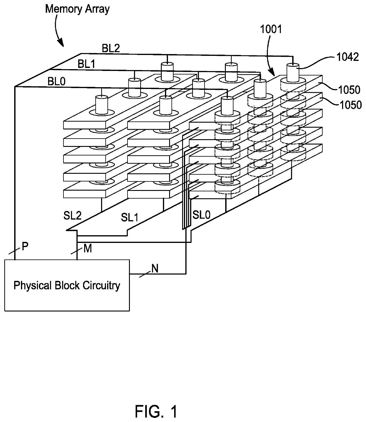
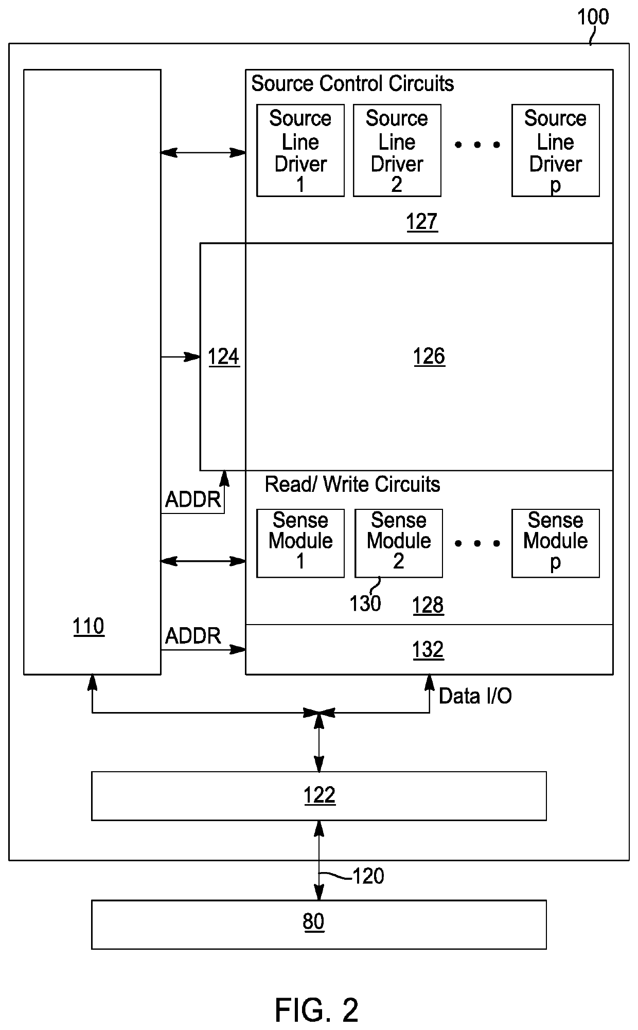
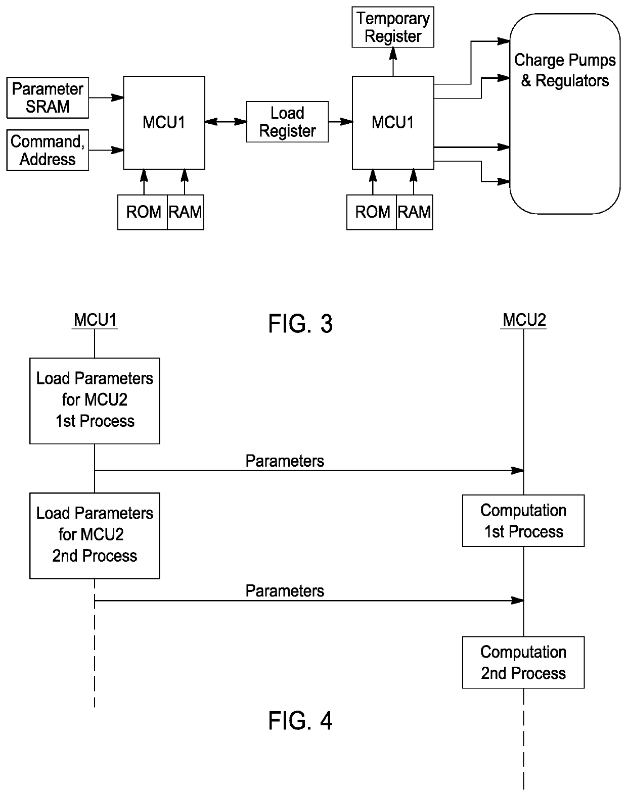
[0040]Reference will now be made in detail to example embodiments which are illustrated in the accompanying drawings, wherein like reference numerals refer to like elements throughout. In this regard, the example embodiments may have different forms and may not be construed as being limited to the descriptions set forth herein.

[0041]It will be understood that the terms “include,”“including”, “comprise, and / or “comprising,” when used in this specification, specify the presence of stated features, integers, steps, operations, elements, and / or components, but do not preclude the presence or addition of one or more other features, integers, steps, operations, elements, components, and / or groups thereof.

[0042]It will be further understood that, although the terms “first,”“second,”“third,” etc., may be used herein to describe various elements, components, regions, layers and / or sections, these elements, components, regions, layers and / or sections may not be limited by these term...


PUM


Abstract

A 3D NAND memory device is provided in which control is performed by two microcontroller units (MCU). During manufacture of the memory device, bug fixes required for the controller may be addressed using a software solution by which an instruction requiring correction in one of the two MCUs is replaced with a corrected instruction stored in a RAM.

Description

TECHNICAL FIELD[0001]Apparatuses and methods consistent with example embodiments relate to control of a three-dimensional (3D) Not-AND (NAND) flash memory using two microcontroller units (MCU), for which bug fixes in manufacturing are addressed using a software solution.DESCRIPTION OF THE RELATED ART[0002]3D NAND flash memory is a type of non-volatile flash memory in which memory cells are stacked vertically in multiple layers. 3D NAND was developed to address challenges encountered in scaling two-dimensional (2D) NAND technology to achieve higher densities at a lower cost per bit.[0003]A memory cell is an electronic device or component capable of storing electronic information. Non-volatile memory may utilize floating-gate transistors, charge trap transistors, or other transistors as memory cells. The ability to adjust the threshold voltage of a floating-gate transistor or charge trap transistor allows the transistor to act as a non-volatile storage element (i.e. a memory cell), su...

Claims


Application Information

Patent Timeline
IPC IPC(8): G06F11/36G11C16/30G06F9/22G06F9/26G06F9/24
CPCG06F11/3648G11C16/30G06F9/24G06F9/261G06F9/226G11C16/0483G06F11/362
Inventor EHAMA, MASAKAZUMIZUKOSHI, HIROYUKILI, YAN
Owner SANDISK TECH LLC
Why Eureka
Try Eureka