Eureka AIR delivers breakthrough ideas for toughest innovation challenges, trusted by R&D personnel around the world.

Quantum Well Structure for Polarized Semiconductors

Pending Publication Date: 2021-07-01
JOHN WASSERBAUER
View PDF2 Cites 0 Cited by
  • Summary
  • Abstract
  • Description
  • Claims
  • Application Information

AI Technical Summary

Benefits of technology

The invention introduces a system to reduce or get rid of polarization effects in a specific device structure. This is achieved by gradually changing the composition of the materials used to create the structure, from one side to the other. The system also involves the use of an electron barrier layer to further improve the device's performance. Overall, this patent aims to improve the efficiency and stability of optical devices made using compound semiconductor quantum wells.

Problems solved by technology

As a consequence, large internal electrical fields appear between heterointerfaces leading to several detrimental effects for optoelectronic devices.
This is known as the quantum confined Stark effect (QCSE) and results in a weaker transition and longer carrier lifetimes, leading to a reduction of the photon emission rate.
This effect makes it difficult to fabricate a practical UV laser from these materials.
An additional drawback to polarized interfaces regards the electron blocking layer (EBL), which is intended to keep energetic electrons from escaping from the active region and recombining in the p-type cladding.
As a result, electron leakage is increased and device efficiency is reduced.
This effect raises the threshold current of lasers and reduces the internal quantum efficiency of both lasers and light emitting diodes (LEDs).

Method used


Image

  • Quantum Well Structure for Polarized Semiconductors
  • Quantum Well Structure for Polarized Semiconductors
  • Quantum Well Structure for Polarized Semiconductors

Examples


Embodiment Construction

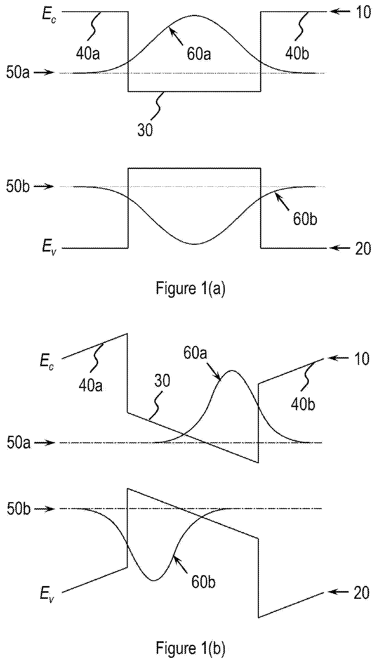
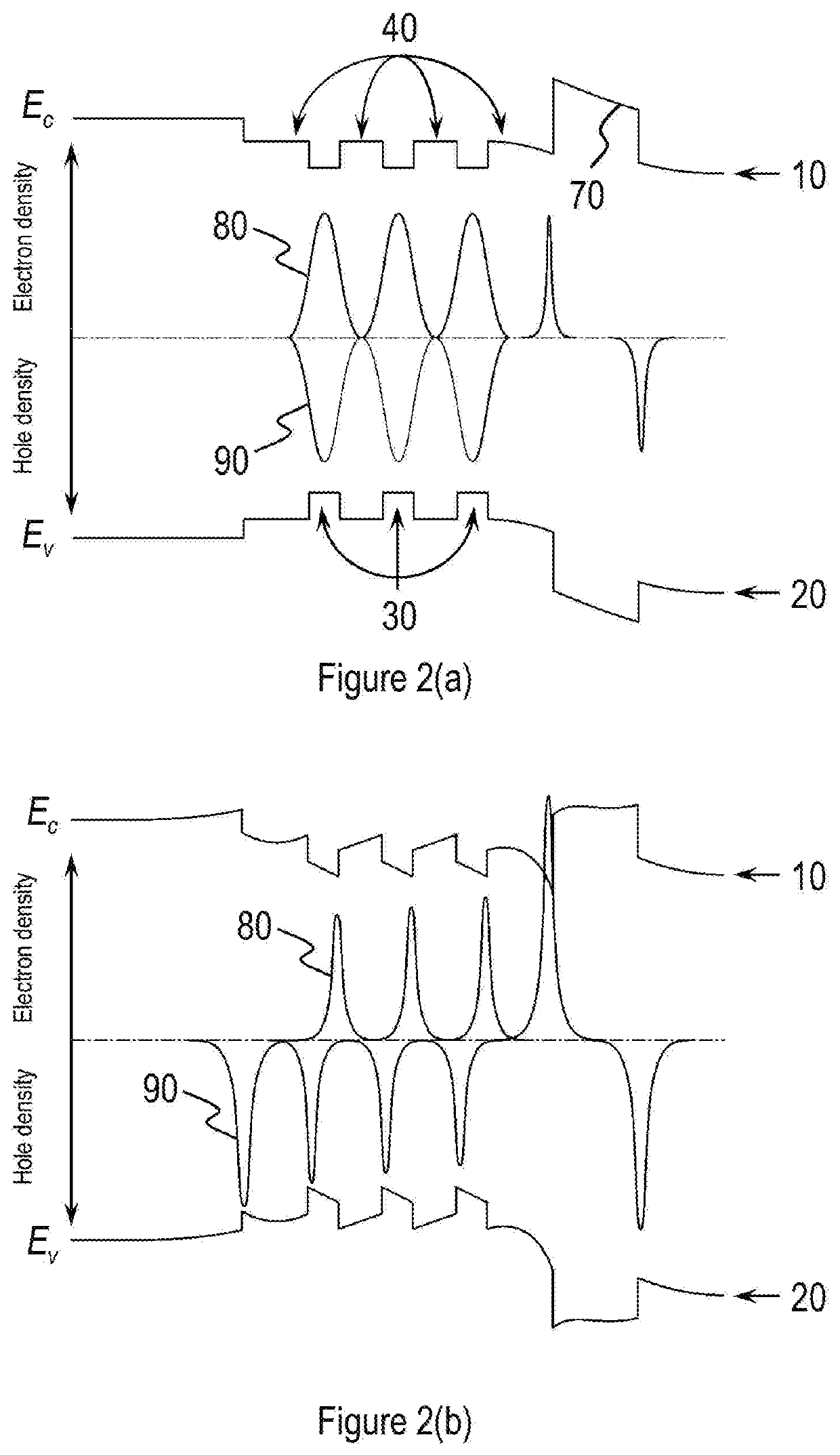
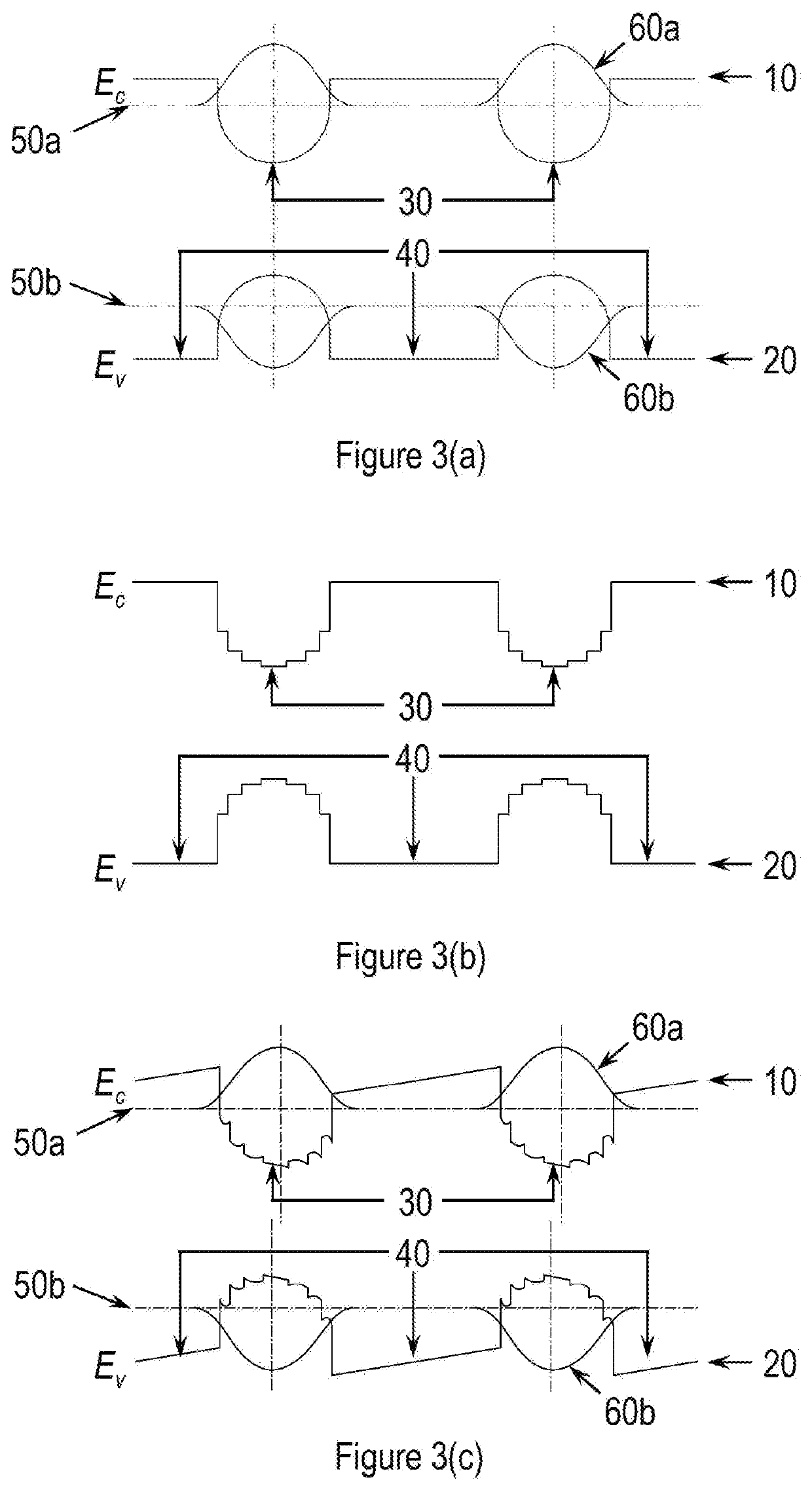
[0016]Non-limiting embodiments of the invention will be described below with reference to the accompanying drawings, wherein like reference numerals represent like elements throughout. While the invention has been described in detail with respect to the preferred embodiments thereof, it will be appreciated that upon reading and understanding of the foregoing, certain variations to the preferred embodiments will become apparent, which variations are nonetheless within the spirit and scope of the invention. The drawings featured in the figures are provided for the purposes of illustrating some embodiments of the invention, and are not to be considered as limitation thereto.

[0017]The invention provides a device, apparatus, system and method for using an interface grading scheme for reducing or eliminating the negative effects of polarization, primarily the quantum confined Stark effect (QCSE) and carrier leakage effect, in a compound semiconductor quantum well structure. Regarding the ...


PUM


Abstract

The invention relates to an apparatus, system and method for reducing or eliminating polarization effects in a compound semiconductor quantum well optical gain structure including the quantum confined Stark effect (QCSE) and carrier leakage effects. The system comprises a quantum well formed by a monotonic, stepwise and / or continuous compositional grading of a first quantum well interface toward a reduced bandgap, also including a monotonic, stepwise or continuous compositional grading of a second quantum well interface toward an increased bandgap thereby creating a quantum well shape that is substantially symmetric under the influence of electrostatic and / or electrodynamic fields. The system also comprises an electron blocking layer formed by a stepwise or continuous compositional grading starting from the maximum bandgap of the quantum well and increasing toward a larger bandgap, thereby creating a barrier shape with reduced electron sheet charge due to the influence of electrostatic fields.

Description

BACKGROUND OF THE INVENTIONField of the Invention[0001]The invention relates to an apparatus, system and method for a quantum well active structure for polarized compound semiconductors, and, more particularly, a quantum well structure that remains substantially symmetric under the influence of electrostatic and / or electrodynamic fields. The invention further relates to a quantum well active structure with an electron blocking layer that does not support a large accumulation of electrons at its quantum well side interface under the influence of electrostatic fields.Background of the Invention[0002]Compound semiconductors have achieved great success in realizing practical optoelectronic devices, such as lasers and detectors. Compounds based on III-V elements, such as InP and GaAs, have produced optoelectronic devices that emit light from the far infrared to visible (orange) wavelengths. For short wavelengths from the green to ultraviolet, larger bandgap semiconductors, such as the II...

Claims


Application Information

Patent Timeline
IPC IPC(8): H01S5/34H01S5/20H01S5/32H01L33/06
CPCH01S5/34H01L33/06H01S5/3216H01S5/2013H01S5/3407H01S5/3408H01S5/2009
Inventor WASSERBAUER, JOHN
Owner JOHN WASSERBAUER
Why Eureka
Eureka Blog
Learn More