Three-dimensional semiconductor memory device and method of fabricating the same
a semiconductor memory and three-dimensional technology, applied in the field of three-dimensional semiconductor memory devices, can solve the problems of the equipment needed to increase the fineness of the pattern, and the practical limitation of increasing the integration of two-dimensional or planar semiconductor devices
- Summary
- Abstract
- Description
- Claims
- Application Information
AI Technical Summary
Benefits of technology
Problems solved by technology
Method used
Image


Examples
Embodiment Construction
[0022]It should be noted that these figures are intended to illustrate the general characteristics of methods, structure and / or materials utilized in certain example embodiments and to supplement the written description provided below. These drawings need not be to scale and might not precisely reflect the precise structural or performance characteristics of any given embodiment, and need not be interpreted as defining or limiting the range of values or properties encompassed by example embodiments. For example, the relative thicknesses and positioning of molecules, layers, regions, and / or structural elements may be reduced or exaggerated for clarity. The use of similar or identical reference numbers in the various drawings may be intended to indicate the presence of a similar or identical element or feature.
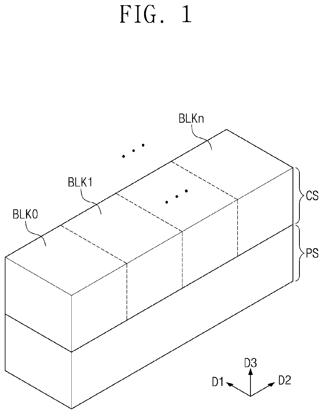
[0023]FIG. 1 is a schematic perspective view illustrating a three-dimensional semiconductor memory device according to an embodiment of the inventive concept.
[0024]Referring to ...
PUM
| Property | Measurement | Unit |
|---|---|---|
| height | aaaaa | aaaaa |
| distance | aaaaa | aaaaa |
| width | aaaaa | aaaaa |
Abstract
Description
Claims
Application Information