Area light source and display device utilizing area light source

Inactive Publication Date: 2021-07-22
WUHAN CHINA STAR OPTOELECTRONICS TECH CO LTD
View PDF0 Cites 0 Cited by
  • Summary
  • Abstract
  • Description
  • Claims
  • Application Information

AI Technical Summary

Benefits of technology

The patent describes an area light source and display device that use double-side die bonds for improved performance. This reduces internal stresses on the substrate and improves uniformity of luminance. The substrates are slightly thicker for better results, and the device uses three-color chips for better control of display without additional films. This results in thinner overall devices.

Problems solved by technology

Polyimide, a substrate material, causes large internal stress during heating, which makes material of the panel greatly curve after reflow weld processes.
As a result, positions of the chips and directions of light emission are affected by the curved material and the subsequent modular assembly process faces a huge challenge.
The thermal characteristics of the materials are unchangeable thus solution has not been found to solve the internal stress caused by die bond.
The structure of double-side display increases the thickness of the display screen and solutions for reducing the thickness of the double-side display have not been found yet.
Thus, uncompleted welding and short circuiting happens, and the subsequent cutting process is affected.

Method used


Image

  • Area light source and display device utilizing area light source
  • Area light source and display device utilizing area light source
  • Area light source and display device utilizing area light source

Examples


Embodiment Construction

[0026]The embodiments of the present disclosure are described in detail below, and the examples of the embodiments are illustrated in the drawings. The same or similar reference numbers are used to refer to the same or similar elements or elements having the same or similar functions. The embodiments described below accompanying with the drawings are illustrative and are only used to explain the present disclosure rather than limiting the present disclosure.

[0027]The following description of the embodiments is provided to illustrate the specific embodiments of the present disclosure may be implemented. Directional terms mentioned in the present disclosure, such as “upper”, “lower”, “front”, “back”, “left”, “right”, “top”, “bottom”, etc., only refer to relative direction in drawings. Therefore, the directional term is used to describe and understand the present disclosure rather than limiting the present disclosure.

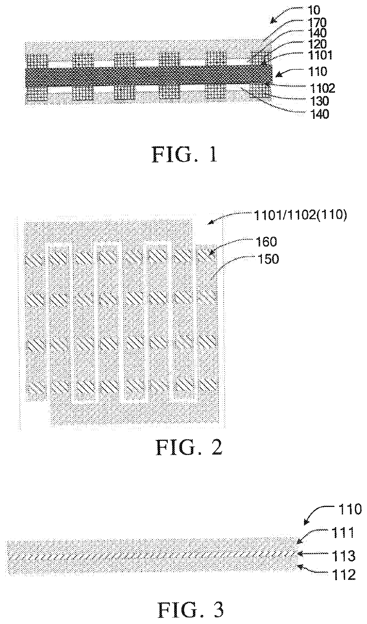
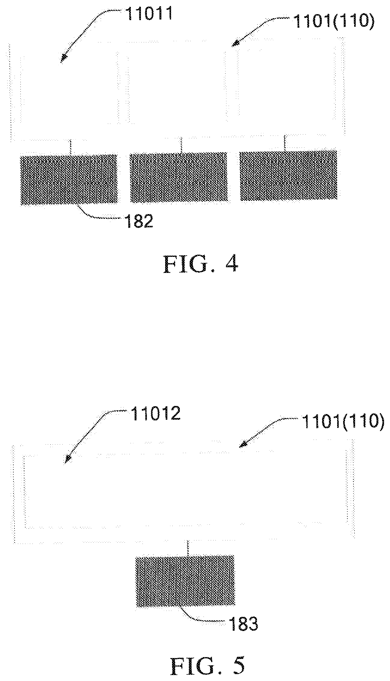
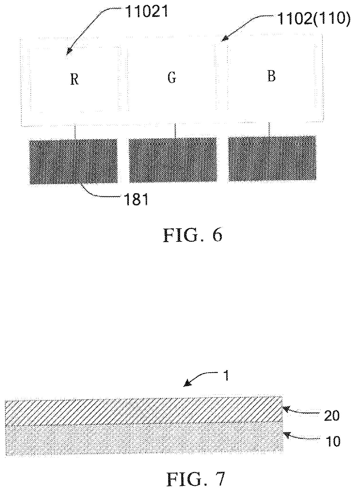
[0028]As shown in FIG. 1, in an embodiment, the area light source 10 ...


PUM


Abstract

The present disclosure discloses an area light source and a display device utilizing the area light source. The area light source includes a substrate including a front surface and a back surface both having weld plates and metal wires. First chips are disposed on the front surface of the substrate and welded to the weld plate. Second chips are disposed on the back surface of the substrate and welded tot the weld plate. The area light source and the display device utilizing the area light source adopt double-side in bound improves curve of the substrate during a reflow process, improves short circuit resulted from chip dragging caused by weld paste, and improves the uniformity of the area light source. Even a thickness of the area light source decreases an entire thickness of the area light source and the display device decreases so the display device is thinner.

Description

FIELD OF INVENTION[0001]The present disclosure relates to fields of display device, more particular, to fields of an area light source and a display device utilizing the area light source.BACKGROUND OF INVENTION[0002]Mini light-emitting diode (LED) display technology is competitive in the future organic light-emitting diode (OLED) display technology market. Research of mini LED display devices become popular because mini LED display devices have advantages such as high brightness, flexibility and bendability, high dynamic contrast display, narrow bezels, special-shaped displays, etc. However, for the purpose of implementing flexible display, most substrates adopt flexible circuit boards. Polyimide, a substrate material, causes large internal stress during heating, which makes material of the panel greatly curve after reflow weld processes. As a result, positions of the chips and directions of light emission are affected by the curved material and the subsequent modular assembly proc...

Claims


Application Information

Patent Timeline
IPC IPC(8): H01L33/12H01L25/075H01L33/62H01L33/60
CPCH01L33/12H01L33/60H01L33/62H01L25/0753G09F9/33G09G3/32H01L25/0756H01L25/167H01L33/50
Inventor YANG, YONG
Owner WUHAN CHINA STAR OPTOELECTRONICS TECH CO LTD
Why Eureka
Try Eureka