Vertical memory devices

Active Publication Date: 2021-09-02
SAMSUNG ELECTRONICS CO LTD
View PDF0 Cites 1 Cited by
  • Summary
  • Abstract
  • Description
  • Claims
  • Application Information

AI Technical Summary

Benefits of technology

[0008]In example embodiments, a dishing defect in which the upper surface of the first insulating interlayer covering an upper portion of the wiring connection structure is recessed may be decreased. Thus

Problems solved by technology

Therefore, when an insulating interlayer covering the pad structure and the cell stacked structure is planarized, a dishing defect of an upper surface of the insulating interlayer may occur.
The

Method used


Image

  • Vertical  memory devices
  • Vertical  memory devices
  • Vertical  memory devices

Examples


Embodiment Construction

[0014]Hereinafter, a direction substantially perpendicular to the upper surface of the substrate is defined as a vertical direction. Two directions substantially parallel to the upper surface of the substrate and crossing to each other are defined as first and second directions, respectively. In example embodiments, the first and second directions may be substantially perpendicular to each other.

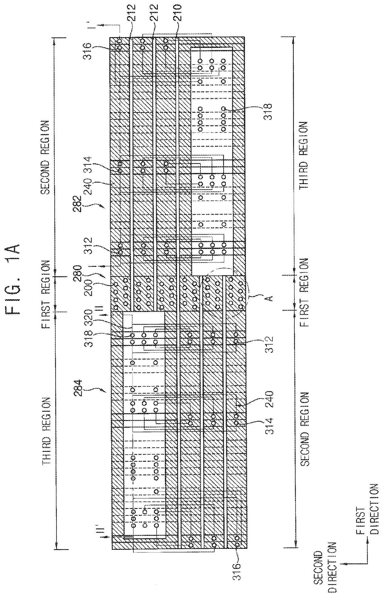
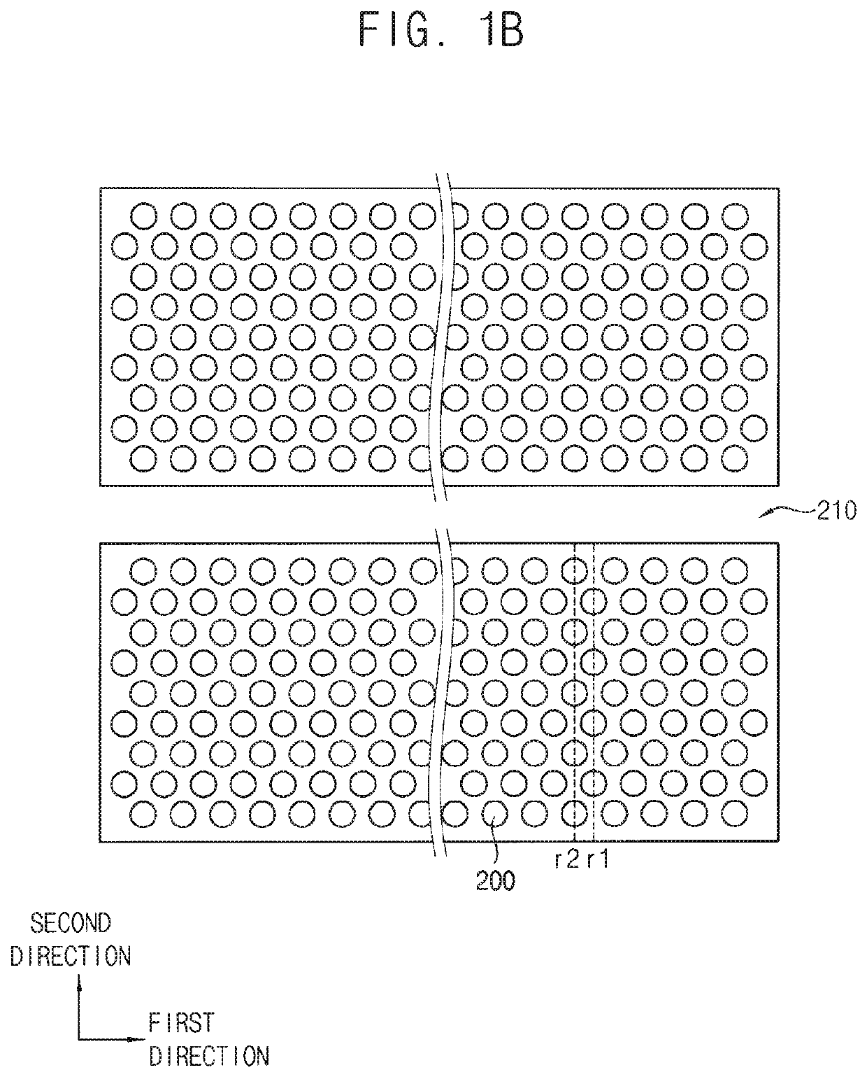
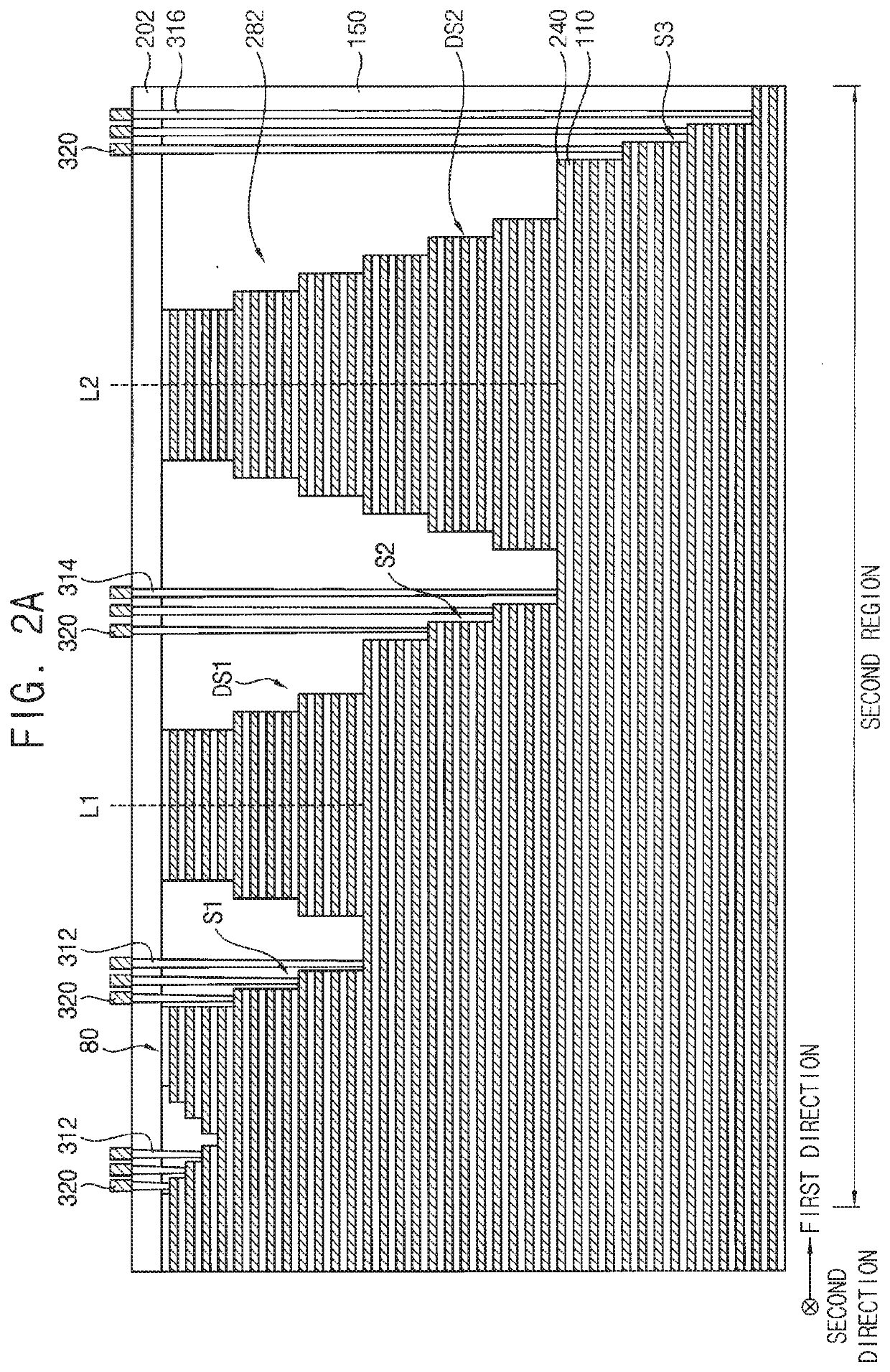
[0015]FIGS. 1A, 1B, 2A, 2B, 3, and 4 are plan views, cross-sectional views, and perspective views illustrating vertical memory devices in accordance with example embodiments. FIG. 5 is a cross-sectional view illustrating a portion of a substrate in the vertical memory devices.

[0016]Particularly, FIGS. 1A and 1B are plan views, FIGS. 2A, 2B and 4 are cross-sectional views, and FIG. 3 is a perspective view.

[0017]FIG. 1B is an enlarged view of a portion A in FIG. 1A. FIG. 2A is the cross-sectional view of a wiring connection structure on a second region cut in the first direction. FIG. 2B is th...


PUM


Abstract

A vertical memory device includes a cell stacked structure, a wiring connection structure, and a first insulating interlayer. The cell stacked structure may include insulation layers and gate patterns repeatedly and alternately stacked on a first region of a substrate. The wiring connection structure may contact side walls of the cell stacked structure. The wiring connection structure may include a first staircase structure having one side of a stepped shape, a second staircase structure having one side of a stepped shape and disposed below the first staircase structure, and a first dummy staircase structure between the first and second staircase structures. The first and second staircase structures may be spaced apart from each other in the first direction, and both sides in the first direction of the first dummy staircase structure may have stepped shapes. The first insulating interlayer may be on the substrate to cover the wiring connection structure.

Description

CROSS-REFERENCE TO RELATED APPLICATION[0001]This application claims priority under 35 USC § 119 to Korean Patent Application No. 10-2020-0024856, filed on Feb. 28, 2020, in the Korean Intellectual Property Office (KIPO), the contents of which are incorporated by reference herein in their entirety.BACKGROUND1. Field[0002]Example embodiments relate to vertical memory devices. More particularly, example embodiments relate to vertical nand (VNAND) flash memory devices.2. Description of the Related Art[0003]A VNAND flash memory device may include a cell stacked structure included in gate patterns of memory cells and a pad structure contacting sidewalls of the cell stacked structure and having a stepped shape. As a stacking height of the memory cells increases, a height of the cell stacked structure may increase and a step difference between the cell stacked structure and the pad structure may increase. Therefore, when an insulating interlayer covering the pad structure and the cell stack...

Claims


Application Information

Patent Timeline
IPC IPC(8): H01L23/528H01L27/11519H01L27/11556H01L27/11565H01L27/11582H01L23/522H01L23/535H01L21/768
CPCH01L23/5283H01L27/11519H01L27/11556H01L27/11565H01L27/11582H01L21/76895H01L23/535H01L21/76805H01L21/76816H01L21/76877H01L23/5226H10B43/35H10B43/50H10B43/10H10B43/27H01L23/49827H10B41/10H10B41/27
Inventor SHIN, SEUNGJUN
Owner SAMSUNG ELECTRONICS CO LTD
Why Eureka
Try Eureka