Sensor package structure

Pending Publication Date: 2021-09-30
TONG HSING ELECTRONICS INDS
View PDF3 Cites 1 Cited by
  • Summary
  • Abstract
  • Description
  • Claims
  • Application Information

AI Technical Summary

Benefits of technology

The present patent provides a sensor package structure that solves issues with conventional structures. It includes a ring-shaped solder mask frame that surrounds the sensor chip, allowing for precise control over the chip's sensing region and preventing contamination during manufacturing. This results in a higher yield rate and throughput.

Problems solved by technology

As the size of the sensor chip becomes smaller, a sensing region of the sensor chip shall be more closer to lateral sides of the sensor chip, and therefore the sensing region is more easily contaminated by the melted or fluid package body (or a sealing gel) during the manufacturing process of the conventional package structure, affecting the production yield or causing product failure.

Method used


Image

  • Sensor package structure
  • Sensor package structure
  • Sensor package structure

Examples


first embodiment

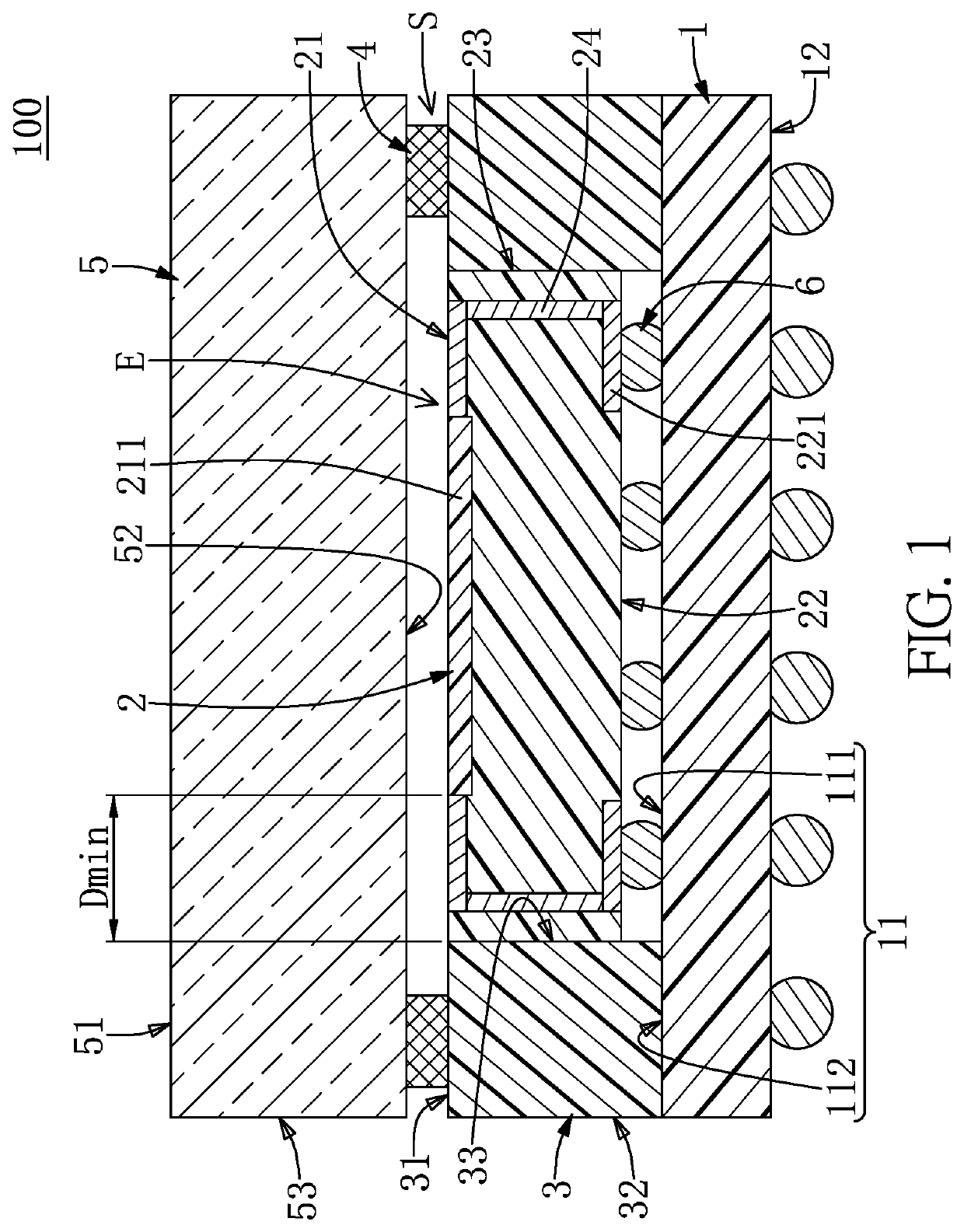
[0019]Referring to FIG. 1, a first embodiment of the present disclosure provides a sensor package structure 100. The sensor package structure 100 includes a substrate 1, a sensor chip 2 disposed on the substrate 1 through a plurality of solder balls 6, a ring-shaped solder mask frame 3 disposed on the substrate 1, a ring-shaped support 4 disposed on the ring-shaped solder mask frame 3, and a light permeable member 5 that is disposed on the ring-shaped support 4. Herein, the sensor package structure 100 in the present embodiment is illustrated as including the above components, but the sensor package structure 100 can be modified according to design requirements.

[0020]It should be noted that in order to conveniently describe the sensor package structure 100 of the present embodiment, FIG. 1 is plotted as a cross-sectional view. It could be understood that some portions of the sensor package structure 100 not shown in FIG. 1 shall have corresponding structures. For example, FIG. 1 sho...

second embodiment

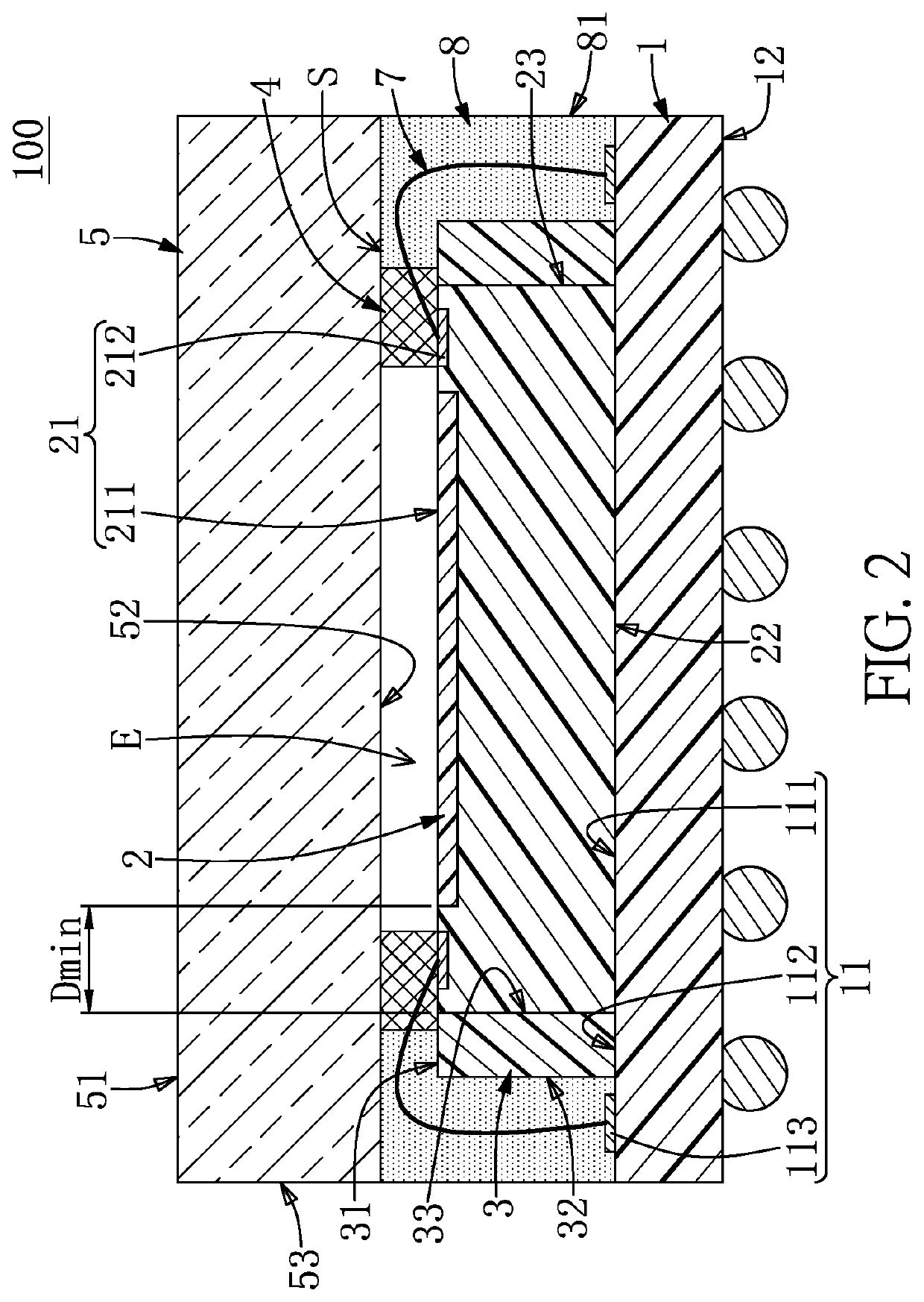
[0029]Referring to FIG. 2, a second embodiment of the present disclosure is disclosed therein. The second embodiment is similar to the first embodiment, so descriptions for identical portions between the two embodiments shall not be repeated again, and the differences between the two embodiments shall be recited in the following.

[0030]In the present embodiment, the sensor package structure 100 includes a substrate 1, a sensor chip 2 disposed on the substrate 1, a ring-shaped solder mask frame 3 disposed on the substrate 1, a ring-shaped support 4 disposed on both the ring-shaped solder mask frame 3 and the sensor chip 2, a light permeable member 5 disposed on the ring-shaped support 4, a plurality of metal wires 7 electrically coupled to the substrate 1 and the sensor chip 2, and a package body 8 that is formed on the substrate 1.

[0031]The substrate 1 includes a plurality of first pads 113 arranged on the first board surface 11. The first pads 113 are located outside of the carrying...

third embodiment

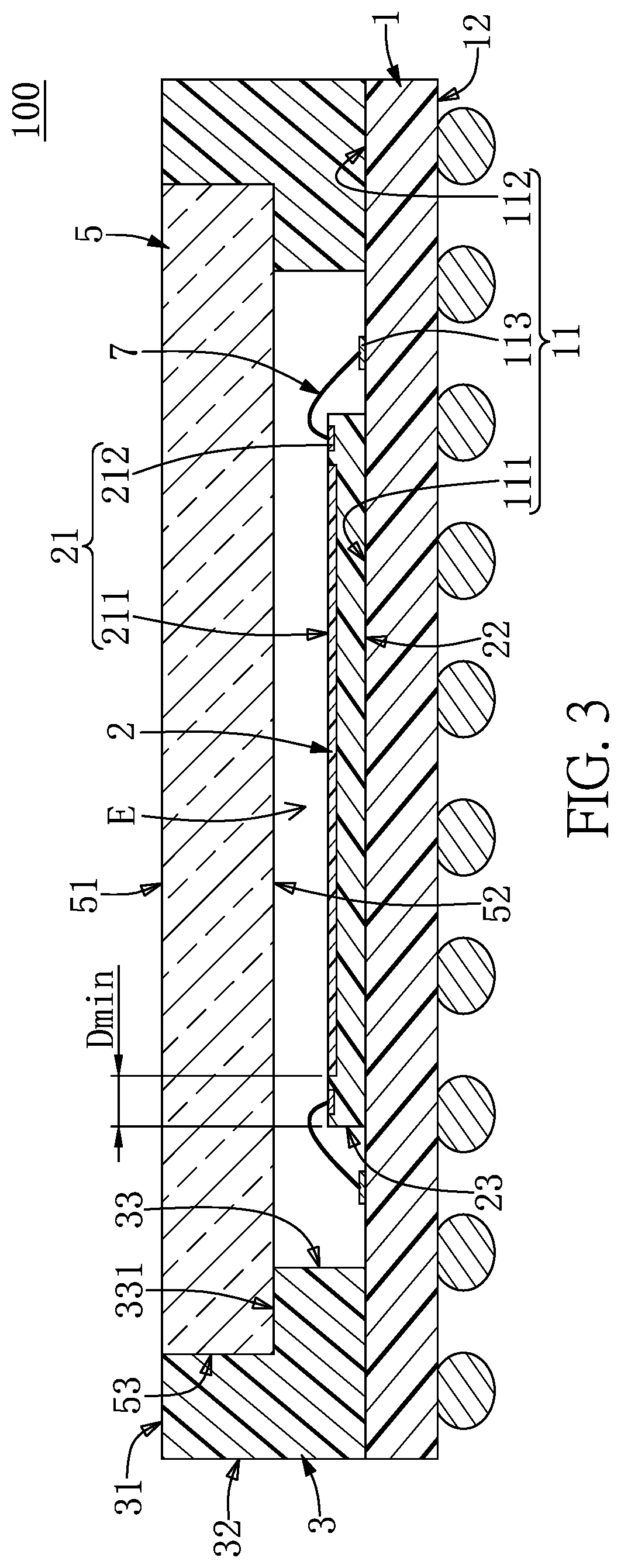
[0035]Referring to FIG. 3 and FIG. 4, a third embodiment of the present disclosure is similar to the first and second embodiments of the present disclosure, so descriptions for identical portions among the embodiments will be not repeated again, and the differences between the first and second embodiments shall be recited in the following.

[0036]In the present embodiment, the ring-shaped solder mask frame 3 is disposed on the carrying region 112 of the first board surface 11 of the substrate 1. The ring-shaped solder mask frame 3 surrounds and is spaced apart from the outer lateral side 23 of the sensor chip 2. In other words, the sensor chip 2 and the metal wires 7 are arranged in a space enclosed by the ring-shaped solder mask frame 3. Moreover, the ring-shaped solder mask frame 3 in the present embodiment is integrally formed as a one-piece structure. The outer lateral side 32 of the ring-shaped solder mask frame 3 is coplanar with the outer lateral side of the substrate 1, and th...


PUM


Abstract

A sensor package structure includes a substrate, a sensor chip and a ring-shaped solder mask frame those are disposed on the substrate, a ring-shaped support disposed on a top side of the annular solder mask frame, and a light permeable member that is disposed on the ring-shaped support. The sensor chip is electrically coupled to the substrate. A top surface of the sensor chip has a sensing region, and the sensing region is spaced apart from an outer lateral side of the sensor chip by a distance less than 300 μm. The ring-shaped solder mask frame surrounds and contacts the outer lateral side of the sensor chip. The light permeable member, the ring-shaped support, and the sensor chip jointly define an enclosed space.

Description

CROSS-REFERENCE TO RELATED PATENT APPLICATION[0001]This application claims the benefit of priority to Taiwan Patent Application No. 109110135, filed on Mar. 26, 2020. The entire content of the above identified application is incorporated herein by reference.[0002]Some references, which may include patents, patent applications and various publications, may be cited and discussed in the description of this disclosure. The citation and / or discussion of such references is provided merely to clarify the description of the present disclosure and is not an admission that any such reference is “prior art” to the disclosure described herein. All references cited and discussed in this specification are incorporated herein by reference in their entireties and to the same extent as if each reference was individually incorporated by reference.FIELD OF THE DISCLOSURE[0003]The present disclosure relates to a package structure, and more particularly to a sensor package structure.BACKGROUND OF THE D...

Claims


Application Information

Patent Timeline
IPC IPC(8): H01L31/02H01L31/0203
CPCH01L31/02002H01L31/0203H01L27/14618
Inventor LIU, FU-CHOUHSU, JUI-HUNGPENG, YU-CHIANGLEE, CHIEN-CHENCHANG, YA-HANHUNG, LI-CHUN
Owner TONG HSING ELECTRONICS INDS
Why Eureka
Try Eureka