Systems and methods for packaging an acoustic device in an integrated circuit (IC)

a technology of integrated circuits and acoustic devices, applied in the direction of impedence networks, electrical devices, etc., can solve the problems of general fragility of acoustic devices, reduce encroachment by encapsulating materials, and reduce the overall size of acoustic devices

Pending Publication Date: 2021-10-07
RF360 SINGAPORE PTE LTD
View PDF0 Cites 1 Cited by
  • Summary
  • Abstract
  • Description
  • Claims
  • Application Information

AI Technical Summary

Benefits of technology

[0004]Aspects disclosed in the detailed description include systems and methods for packaging an acoustic device in an integrated circuit (IC). In an exemplary aspect, an IC is provided that includes an IC chip that includes an acoustic device. The IC is coupled to a wiring substrate to provide connectivity to the IC chip and its acoustic device. For example, the acoustic device may be used as a filter. The IC chip is encapsulated. In exemplary aspects, the IC chip includes walls formed on a wiring substrate. The walk have a height, which is shorter than an expected height of a solder bump on an acoustic device after solder reflow. The walls are positioned on either side of the acoustic device and a small portion lies underneath an exterior edge of the acoustic device such that a relatively small gap is formed between an upper surface of the walls and the lower surface of the acoustic device. By providing a small gap between the walls and the acoustic device, encroachment by an encapsulating material into a keep out zone of the acoustic device is minimized. Reduction of encroachment allows more area within the acoustic device to be used for acoustic elements, which reduces an overall size of the acoustic device.

Problems solved by technology

Acoustic devices are generally fragile and accordingly there is always a need for improved packaging options for acoustic devices.

Method used


Image

  • Systems and methods for packaging an acoustic device in an integrated circuit (IC)
  • Systems and methods for packaging an acoustic device in an integrated circuit (IC)
  • Systems and methods for packaging an acoustic device in an integrated circuit (IC)

Examples


Embodiment Construction

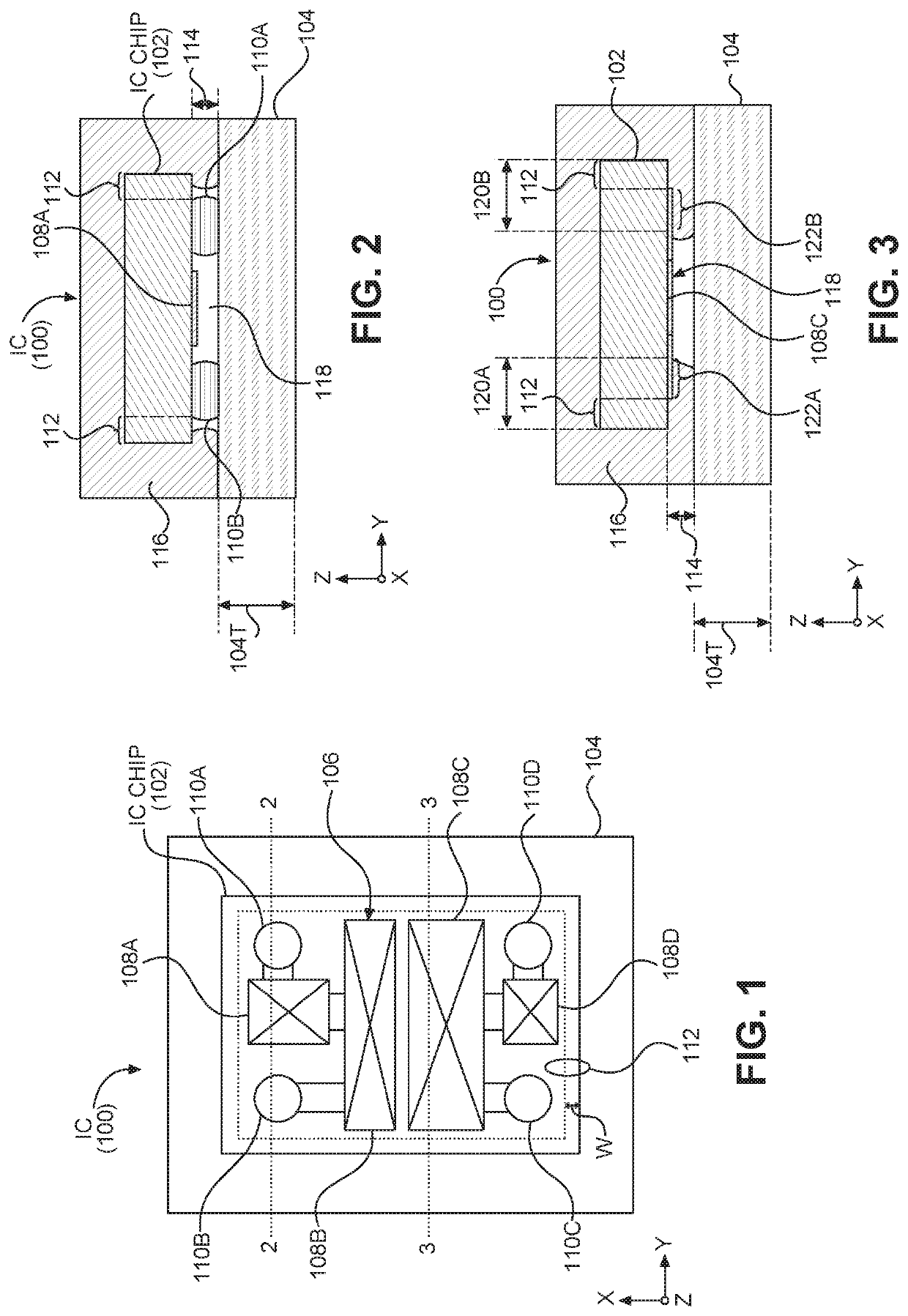
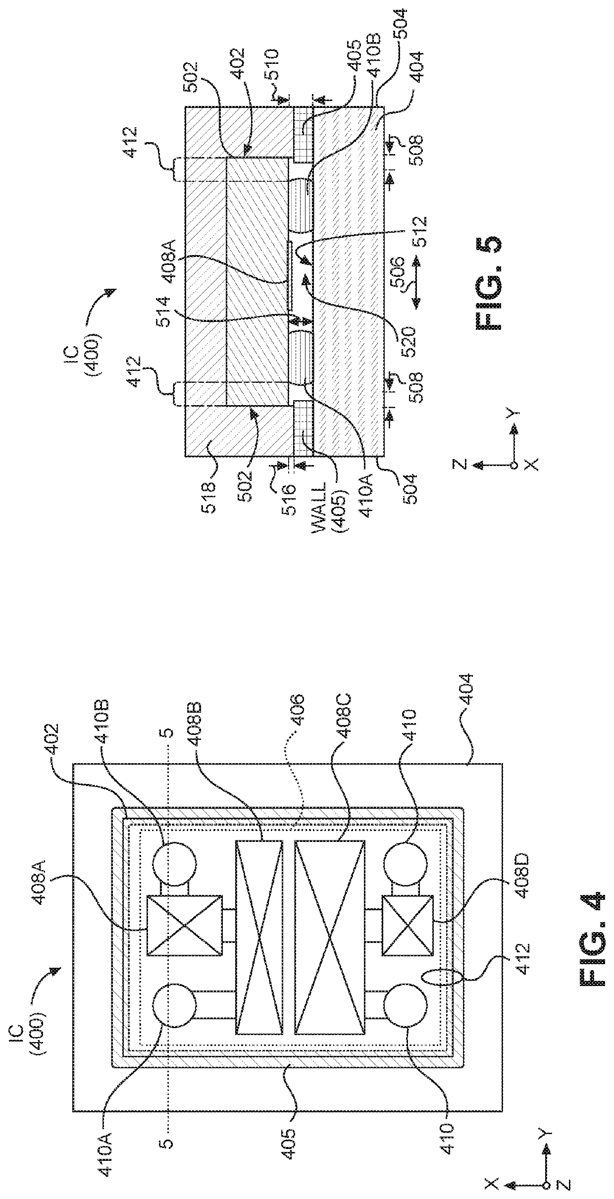
[0023]With reference now to the drawing figures, several exemplary aspects of the present disclosure are described. The word “exemplary” is used herein to mean “serving as an example, instance, or illustration.” Any aspect described herein as “exemplary” is not necessarily to be construed as preferred or advantageous over other aspects.

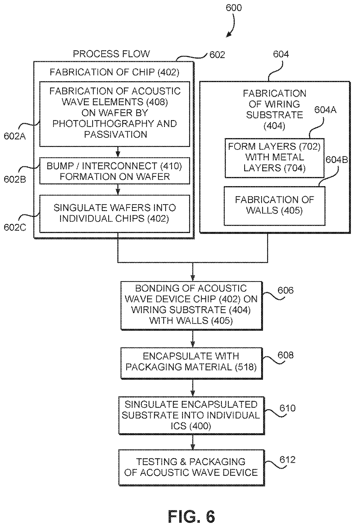
[0024]Aspects disclosed in the detailed description include systems and methods for packaging an acoustic device in an integrated circuit (IC). In an exemplary aspect, an IC is provided that includes an IC chip that includes an acoustic device. The IC is coupled to a wiring substrate to provide connectivity to the IC chip and its acoustic device. For example, the acoustic device may be used as a filter. The IC chip is encapsulated. In exemplary aspects, the IC chip includes walls formed on a wiring substrate. The walls have a height, which is shorter than an expected height of a solder bump on an acoustic device after solder reflow. The walls are posi...


PUM


Abstract

Systems and methods for packaging an acoustic device in an integrated circuit (IC) include walls formed on a wiring substrate. The walls have a height which is just shorter than an expected height of a solder bump on the acoustic device after solder reflow. The walls are positioned on either side of the acoustic device and a small portion lies underneath an exterior edge of the acoustic device such that a relatively small gap is formed between an upper surface of the wall and the lower surface of the acoustic device. By providing a small gap between wall and acoustic device, encroachment by an encapsulating material into a keep out zone of the acoustic device is minimized.

Description

PRIORITY CLAIM[0001]The present application claims priority to U.S. Provisional Patent Application Ser. No. 63 / 005,760 filed on Apr. 6, 2020 and entitled “SYSTEMS AND METHODS FOR PACK AGING AN ACOUSTIC DEVICE IN AN INTEGRATED CIRCUIT (IC),” the contents of which is incorporated herein by reference in its entirety.I. BACKGROUNDField of the Disclosure[0002]The technology of the disclosure relates generally to encapsulating integrated circuits (ICs) and, more particularly, to encapsulating ICs having acoustic devices therein.II. Background[0003]Most mobile communication devices include a radio frequency front end formed from a number of integrated circuits (ICs). These ICs may have different functions such as amplifiers, filters, duplexers, diplexers, and the like. Duplexers and diplexers in particular are useful for operating at different frequency bands or separating transmitted signals from received signals. One of the most effective devices to separate signals at current frequencie...

Claims


Application Information

Patent Timeline
Patent Type & Authority Applications(United States)
IPC IPC(8): H03H9/17H03H3/08
CPCH03H9/176H03H3/08H03H3/02H03H9/1014H03H9/1064H03H9/059H03H9/0523
Inventor KU, HUAN ENYAM, JOO SHANLEE, CHEE KONG
Owner RF360 SINGAPORE PTE LTD
Why Eureka
Try Eureka