Display panel and manufacturing method for display panel

a manufacturing method and display panel technology, applied in the field of display, can solve the problems of reduced partial undesirable alignment, complicated middle-end cell process, and increased flow speed, so as to increase yield, increase competitiveness of products, and ensure the effect of yield and quality

Inactive Publication Date: 2021-10-28
SHENZHEN CHINA STAR OPTOELECTRONICS TECH CO LTD
View PDF0 Cites 0 Cited by
  • Summary
  • Abstract
  • Description
  • Claims
  • Application Information

AI Technical Summary

Benefits of technology

[0018]The technical effect of the present invention is to provide a display panel and a manufacturing method for the display panel, which disposes a first liquid crystal alignment monomer layer on the surface of a common electrode layer, and uses a heat gun to perform heat and light treatment to a color filter substrate to make a link reaction occur between the first liquid crystal alignment monomer layer and the common electrode layer and form a first alignment film layer, and thereby undesirable alignment is improved and greyscale difference of a display panel caused by undesirable alignment is avoided to ensure yields and quality of products. Besides, when manufacturing a color filter substrate, the present invention cuts out a polyimide coating process, and cuts out a rubbing process to avoid drawbacks introduced therefrom, and further increases yields and increases competitiveness of products.

Problems solved by technology

The middle-end cell process is complicated, and during the course of alignment, a heating plate is required to perform heat treatment to mother board of the array substrate.
After heating the mother board of the array substrate, viscosity of the liquid crystal decreases and flow speed increases such that the liquid crystal is aligned and partial undesirable alignment is decreased.
However, undesirable alignment of the liquid crystal cannot be completely overcome, which therefore leads to non-uniform display and an affected yield.

Method used


Image

  • Display panel and manufacturing method for display panel
  • Display panel and manufacturing method for display panel

Examples


Embodiment Construction

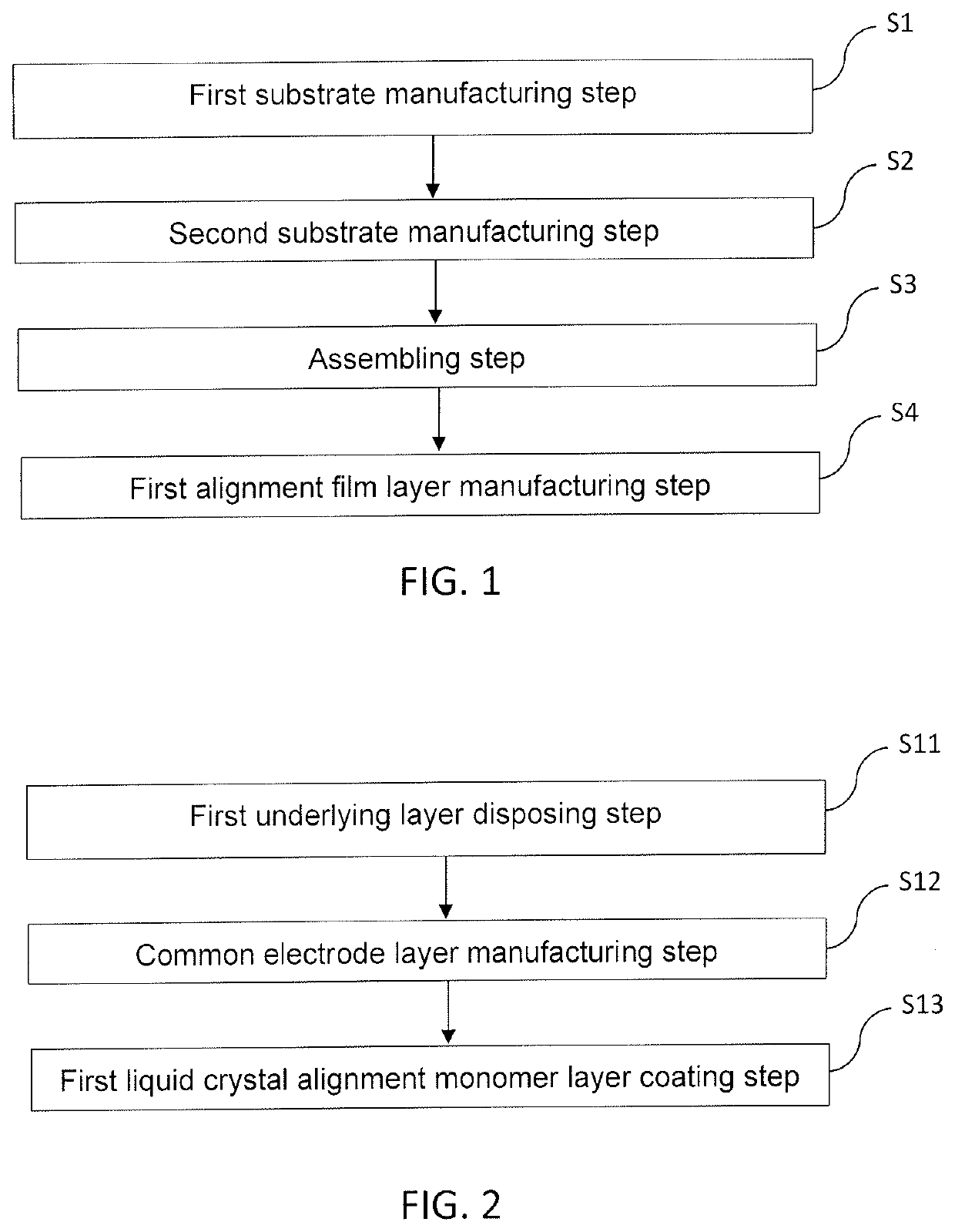
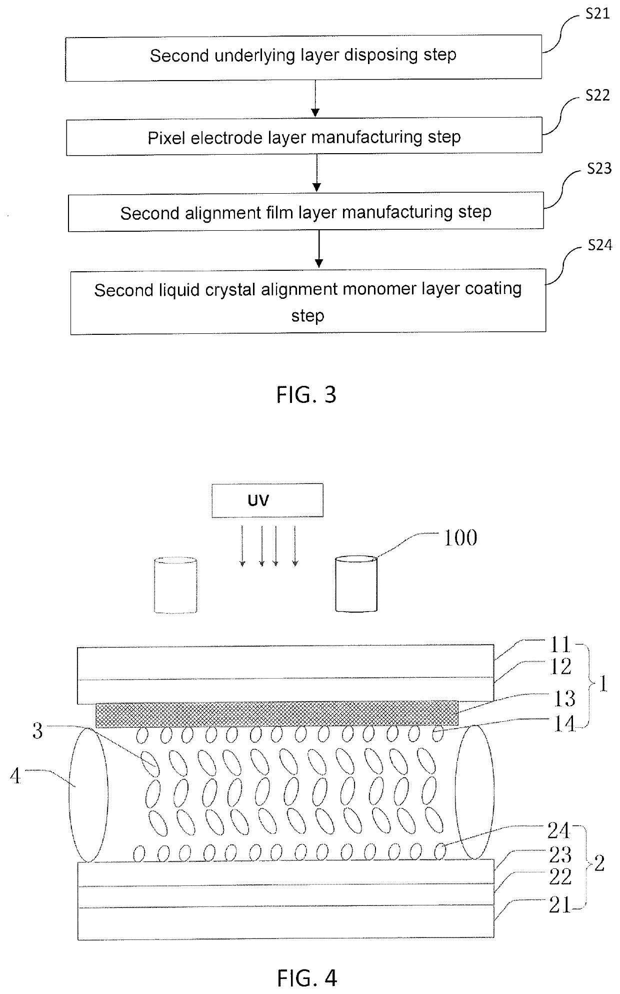
[0025]The embodiments of the present invention are described in detail hereinafter. Examples of the described embodiments are given in the accompanying drawings. It should be noted that, the following embodiments are intended to illustrate and interpret the present invention, which shall not be construed as causing limitations to the present invention. Similarly, the following embodiments are part of the embodiments of the present invention and are not the whole embodiments, and all other embodiments those skilled in the art obtain without making any inventive efforts are within the scope protected by the present invention.

[0026]Terms such as “first”, “second”, etc. (if they exist) in the specification, claim and above-mentioned drawings of the present invention are used herein for purposes of description and are not intended to indicate or imply relative order or significance. It should be understood that elements described by such terms can be switched under proper conditions. Bes...


PUM

PropertyMeasurementUnit
liquid crystal alignmentaaaaaaaaaa
voltageaaaaaaaaaa
electric fieldaaaaaaaaaa

Abstract

A manufacturing method for a display panel that includes the following steps: a first substrate manufacturing step, a second substrate manufacturing step, an assembling step, and a first alignment film layer manufacturing step. The display panel includes a first substrate, a second substrate, a liquid crystal layer, and a sealant layer. The manufacturing method for the display panel disposes a first liquid crystal alignment monomer layer on a surface of a common electrode layer, and uses a heat gun to perform heat and light treatment to a color filter substrate to make a link reaction occur between the first liquid crystal alignment monomer layer and the common electrode layer and form a first alignment film layer, and thereby undesirable alignment is improved and greyscale difference of a display panel caused by undesirable alignment is avoided to ensure yields and quality of products.

Description

FIELD OF INVENTION[0001]The present invention relates to the field of display, and especially to a display panel and a manufacturing method for the display panel.BACKGROUND OF INVENTION[0002]With advantages such as a thin body, power saving, etc., liquid crystal displays (LCDs) have achieved a wide range of applications. LCDs in the market now are mostly backlight LCD panels, which include an LCD panel and a backlight module.[0003]An LCD panel usually includes a thin film transistor (TFT) array substrate, a pixel electrode, a first polyimide (PI) alignment film, a liquid crystal layer, a second polyimide alignment film, a common electrode, and a color filter (CF) substrate. When voltage is applied to the pixel electrode and the common electrode, an electric field is generated in the liquid crystal layer. The electric field determines orientation of liquid crystal molecules, and therefore adjusts polarization of incident light on the liquid crystal layer to produce pictures on the LC...

Claims


Application Information

Patent Timeline
Patent Type & Authority Applications(United States)
IPC IPC(8): G02F1/1337G02F1/1339
CPCG02F1/133788G02F1/133723G02F1/1339G02F1/133516G02F1/1333G02F1/1303G02F1/1337G02F1/1343C09K2219/03G02F1/133715
Inventor XIE, KECHENG
Owner SHENZHEN CHINA STAR OPTOELECTRONICS TECH CO LTD
Why Eureka
Try Eureka