Method for packaging semiconductor, semiconductor package structure, and package

a technology for semiconductors and packaging, applied in semiconductor devices, semiconductor/solid-state device details, electrical devices, etc., can solve the problems of poor reliability of the package structure, the negative effect the inability to reduce the package height, so as to improve the reliability of the package structure, the stability of the semiconductor die stack 210, and the semiconductor package structure can be greatly reduced

Pending Publication Date: 2021-10-28
CHANGXIN MEMORY TECH INC
View PDF0 Cites 0 Cited by
  • Summary
  • Abstract
  • Description
  • Claims
  • Application Information

AI Technical Summary

Benefits of technology

[0028]Advantages of the present disclosure are as below. A groove is formed on the substrate wafer to accommodate the semiconductor die stack, and the semiconductor die stack is sealed up by an insulating dielectric layer. The height of the semiconductor package structure can be greatly reduced while the same number of semiconductor dies is packaged, such that ultra-thin packaging can be achieved. In addition, the insulating dielectric layer covers the upper surface of the semiconductor die stack, and the insulating dielectric layer fills the upper part of the gap between the sidewall of the groove and the semiconductor die stack. While sealing up the semiconductor die stack, the insulating dielectric layer can also fix the semiconductor die stack, such that the semiconductor die stack 210 can be prevented from moving with respect to the substrate wafer 200 even though the semiconductor package structure moves or vibrates. That is, the stability of the semiconductor die stack 210 is improved. Furthermore, a poor connection between the semiconductor dies 210A and a poor connection between the semiconductor die stack 210 and the substrate wafer 200 caused by the movement of the semiconductor die stack 210 can be prevented. That is, the reliability of the semiconductor package structure is improved.

Problems solved by technology

Furthermore, when a semiconductor package structure moves or vibrates, there may likely exist slight translocation between the chips, which results in poor reliability of a package structure and has a negative effect on the performance of the package structure.
Therefore, how to reduce the package height of the package and improve the reliability of the package has become a technical problem urgently needing to be solved at present.

Method used


Image

  • Method for packaging semiconductor, semiconductor package structure, and package
  • Method for packaging semiconductor, semiconductor package structure, and package
  • Method for packaging semiconductor, semiconductor package structure, and package

Examples


Embodiment Construction

[0033]Embodiments of a method for packaging a semiconductor, a semiconductor package structure and a package provided by the present disclosure are described below in detail with reference to the accompanying drawings.

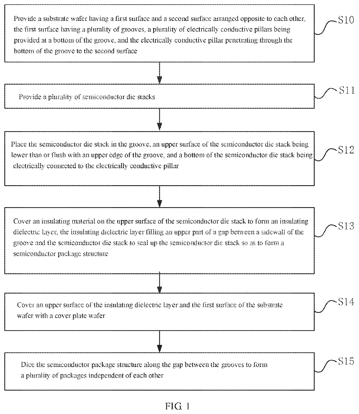
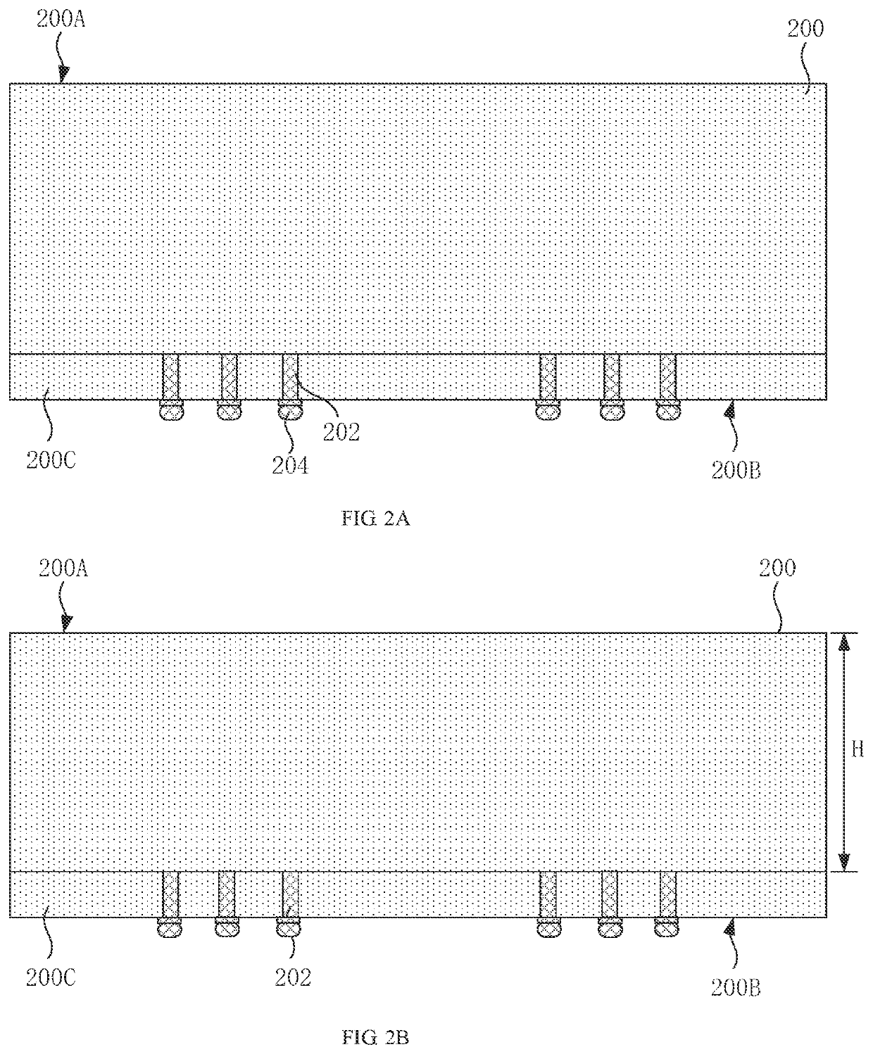
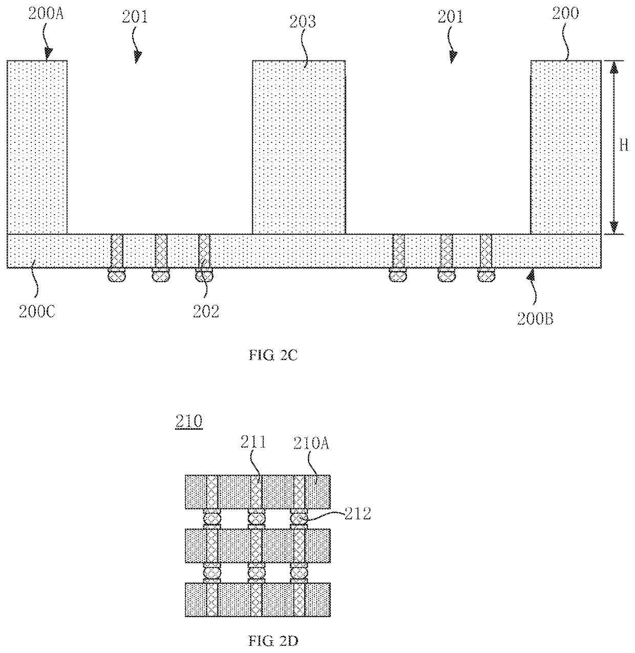
[0034]FIG. 1 is a schematic diagram showing steps of the method for packaging a semiconductor according to one embodiment of the present disclosure. Referring to FIG. 1, the method for packaging a semiconductor includes following steps. In Step S10, a substrate wafer is provided, and the substrate wafer has a first surface and a second surface arranged opposite to each other, wherein the first surface has a plurality of grooves, a plurality of electrically conductive pillars are provided at a bottom of the groove, and the electrically conductive pillar penetrates through the bottom of the groove to the second surface. In Step S11, a plurality of semiconductor die stacks are provided. In Step S12, the semiconductor die stack is placed in the groove, wherein an upper sur...


PUM

PropertyMeasurementUnit
electrically conductiveaaaaaaaaaa
thermal expansion coefficientaaaaaaaaaa
insulatingaaaaaaaaaa

Abstract

Embodiments provide a method for packaging a semiconductor, a semiconductor package structure, and a package. The packaging method includes: providing a substrate wafer having a first surface and a second surface arranged opposite to each other, the first surface having a plurality of grooves, a plurality of electrically conductive pillars being provided at a bottom of the groove, and the electrically conductive pillar penetrating through the bottom of the groove to the second surface; providing a plurality of semiconductor die stacks; placing the semiconductor die stack in the groove, an upper surface of the semiconductor die stack being lower than or flush with an upper edge of the groove, and a bottom of the semiconductor die stack being electrically connected to the electrically conductive pillar; and providing an insulating material on the semiconductor die stack to form a semiconductor package structure.

Description

CROSS REFERENCE TO RELATED APPLICATION[0001]This application is a continuation of PCT / CN2020 / 096258, filed on Jun. 16, 2020, which claims priority to Chinese Patent Application No. 201910982067.2, titled “METHOD FOR PACKAGING SEMICONDUCTOR, SEMICONDUCTOR PACKAGE STRUCTURE, AND PACKAGE” and filed on Oct. 16, 2019, the entire contents of which are incorporated herein by reference.FIELD OF THE INVENTION[0002]The present disclosure relates to the field of semiconductor package, and more particularly, to a method for packaging a semiconductor, a semiconductor package structure, and a package.BACKGROUND OF THE INVENTION[0003]Also known as a 3D or three-dimensional packaging technology, a stacked packaging technology is one of current mainstream multi-chip packaging technologies, which can stack at least two semiconductor chips (also referred to as dies, i.e., blocks having full functions diced from a wafer). The stacked packaging technology is generally employed to manufacture electronic ...

Claims


Application Information

Patent Timeline
Patent Type & Authority Applications(United States)
IPC IPC(8): H01L25/065H01L23/00H01L21/78H01L25/00
CPCH01L25/0657H01L23/562H01L21/78H01L2225/06586H01L2225/06513H01L2225/06541H01L2225/06548H01L25/50H01L25/105H01L2225/06517H01L23/16H01L2224/06181H01L2924/15311H01L2225/06565H01L2224/0401H01L2224/0557H01L2224/16235H01L2225/1094H01L2224/17181H01L2224/73204H01L2224/32225H01L24/73H01L24/32H01L24/06H01L24/05H01L24/16H01L24/17H01L23/055H01L2224/16146H01L2224/81192H01L2224/83903H01L2224/83191H01L2224/29006H01L2224/32105H01L2224/32106H01L24/29H01L24/13H01L2224/13025H01L24/97H01L2224/95H01L2224/83901H01L24/81H01L24/83H01L2924/15153H01L23/49827H01L23/49816H01L23/49833H01L23/3677H01L2224/16225H01L2924/00H01L2224/81H01L2224/83H01L2924/00012
Inventor LIU, JIEYING, ZHAN
Owner CHANGXIN MEMORY TECH INC
Why Eureka
Try Eureka