

Display device
a technology of display device and display screen, which is applied in the direction of identification means, semiconductor devices, instruments, etc., to achieve the effect of improving the light receiving effect of optical sensing modules
- Summary
- Abstract
- Description
- Claims
- Application Information
AI Technical Summary
Benefits of technology
Problems solved by technology
Method used
Image

Examples
first embodiment
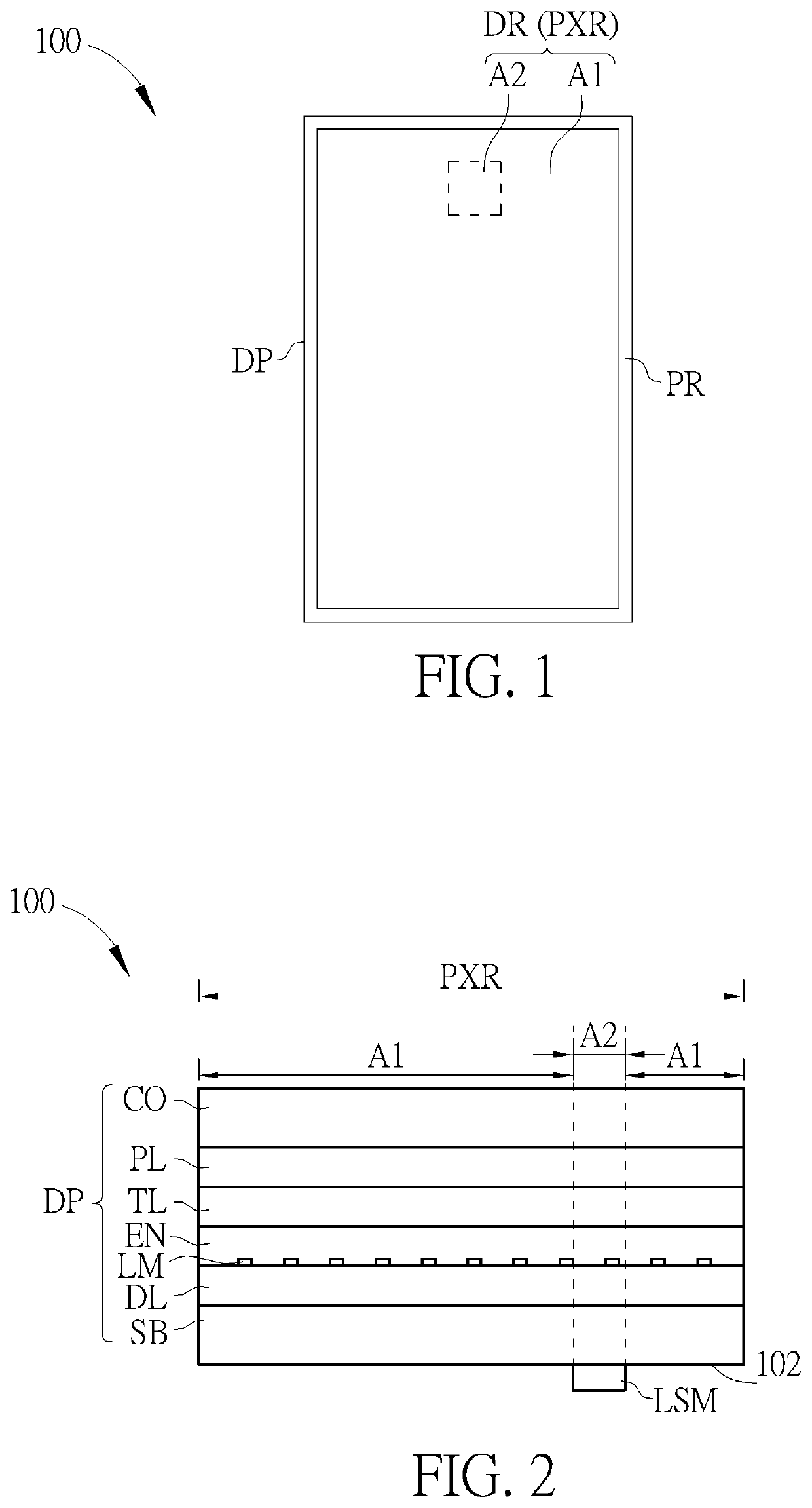
[0024]Referring to FIG. 1, FIG. 1 schematically illustrates a top view of an electronic device according to the present disclosure. The electronic device of the present disclosure may for example include a display device, a light emitting device, a sensing device, a touch display device, a curved display device or a free shape display device, but not limited thereto. The electronic device may be a foldable electronic device or a flexible electronic device. The electronic device may for example include light emitting diode, fluorescence, phosphor, other suitable display mediums or the combinations of the above-mentioned materials, but not limited thereto. The light emitting diode may for example include organic light emitting diode (OLED), mini light emitting diode (mini LED), micro light emitting diode (micro LED), quantum dot light emitting diode (QLED or QDLED), other suitable materials or the combinations of the above-mentioned materials, but not limited thereto. The display devi...
second embodiment
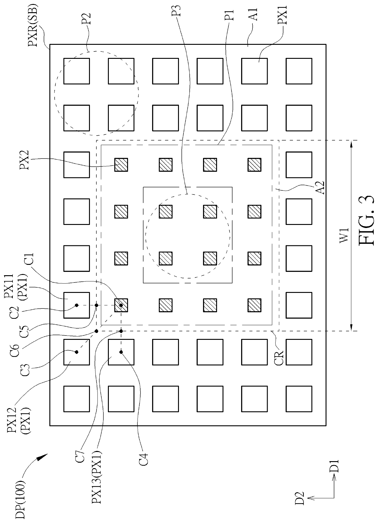
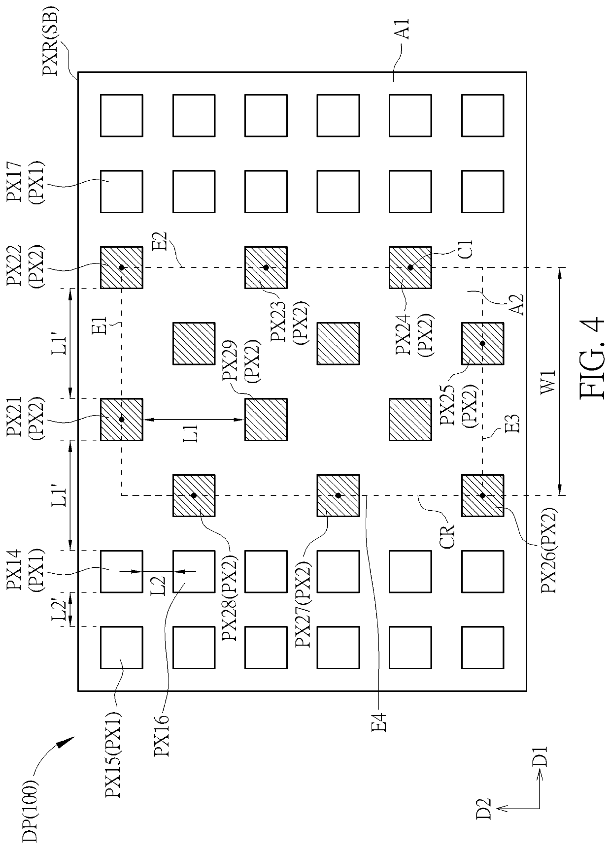
[0034]Referring to FIG. 7, FIG. 7 schematically illustrates the distribution of pixels of an electronic device according to the present disclosure. In order to simplify the figure, FIG. 7 only shows the distribution of the pixels of the display panel DP, and other elements or layers are omitted and may refer to FIG. 2, but not limited thereto. In addition, FIG. 7 show the condition that the display panel DP includes the pixels emitting lights of a single color, but the present disclosure is not limited thereto. One of the main differences between the display panel shown in FIG. 7 and the display panel shown in FIG. 3 is the design of the pixels. According to the present embodiment, the display panel DP may not include the pixel PX2 mentioned in the above-mentioned embodiments and variant embodiments. However, the display panel DP may further include adjusting pixels disposed in the pixel region PXR. In detail, as shown in FIG. 7, the pixel region PXR of the display panel DP of the p...
third embodiment
[0038]Referring to FIG. 9, FIG. 9 schematically illustrates a cross-sectional view of an electronic device according to the present disclosure. In order to simplify the figure, the non-display region of the display device is omitted in FIG. 9, but the present disclosure is not limited thereto. According to the present embodiment, as shown in FIG. 9, the display device 100 may include the display panel DP and the optical sensing module LSM, wherein the display panel DP shown in FIG. 9 and the elements or the layers included in the display panel DP may be the same or similar to the display panel DP shown in FIG. 2, and will not be redundantly described here. In the present embodiment, the optical sensing module LSM may be disposed on the surface of the substrate SB. In detail, as shown in FIG. 9, the display device 100 of the present embodiment may further include a supporting layer SUP and an adhesive layer AD. The supporting layer SUP may provide the supporting function in the displ...
PUM
| Property | Measurement | Unit |
|---|---|---|
| width | aaaaa | aaaaa |
| width | aaaaa | aaaaa |
| width | aaaaa | aaaaa |
Abstract
Description
Claims
Application Information