Organic light emitting diode display panel

a technology display panels, which is applied in the field of display technology, can solve the problems of lowering affecting the product yield, and breaking signals during the manufacturing process, so as to improve the product yield improve the shipment rate of organic light-emitting diodes display panels, and improve the display quality of organic light-emitting

Inactive Publication Date: 2021-11-18
WUHAN CHINA STAR OPTOELECTRONICS SEMICON DISPLAY TECH CO LTD
View PDF0 Cites 0 Cited by
  • Summary
  • Abstract
  • Description
  • Claims
  • Application Information

AI Technical Summary

Benefits of technology

[0004]The technical problem solved by the present application is how to improve the display quality of the organic light emitting diode display panel, thereby improving the product yield of the organic light emitting diode display panel, and improving the shipment rate of the organic light emitting diode display panel.
[0036]By providing at least one spare line on the substrate, when any of the signal lines is disconnected, the disconnected signal line works normally through the spare line to achieve the objective of improving the display quality of the organic light emitting diode display panel, thereby improving the product yield of the organic light emitting diode display panel, and improving the shipment rate of the organic light emitting diode display panel.

Problems solved by technology

In general OLED display panels, since the distance between the signal lines is small, there is a risk that the signal lines will be broken during the manufacturing process.
When the signal line is broken, it will affect the display quality of the OLED display panel, which will result in dropping the yield of the product and lowering the shipment rate of the OLED display panel.

Method used


Image

  • Organic light emitting diode display panel
  • Organic light emitting diode display panel
  • Organic light emitting diode display panel

Examples


first embodiment

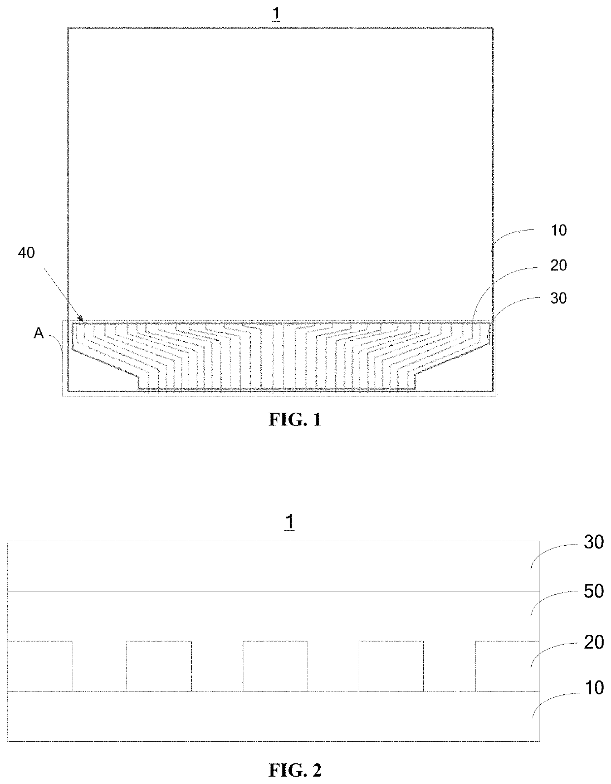
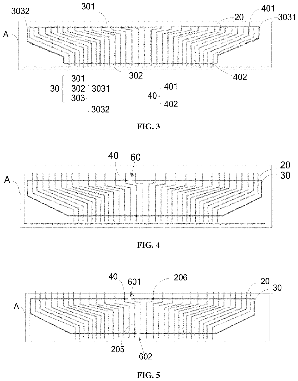
[0052]In some embodiments, the spare line 30 is a ring structure. Please refer to FIG. 3. FIG. 3 is an enlarged view diagram of a portion A of the OLED display panel provided by the present application. The spare line 30 includes a first portion 301 and a second portion 302, and a projection of each of the signal lines 20 on the substrate 10 intersects the first portion 301 and the second portion 302, and the first portion 301 and the second portion 302 are disposed opposite to each other.

[0053]The spare line 30 includes the first portion 301 and the second portion 302, which are disposed opposite to each other. The projection of each of the signal lines 20 on the substrate 10 intersects the first portion 301 and the second portion 302. For instance, when only one spare line 30 is provided, the projection of any of the signal lines 20 on the substrate 10 intersects a projection of the first portion 301 on the substrate 10, and the projection of any of the signal lines 20 on the subs...

second embodiment

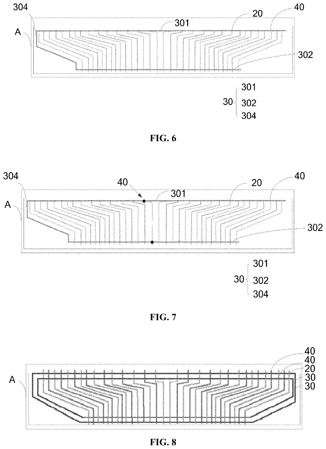
[0061]Please refer to FIG. 6. FIG. 6 is an enlarged view diagram of a portion A of the OLED display panel provided by the present application. The OLED display panel 1 of FIG. 6 differs from the OLED display panel 1 of FIG. 3 in that the spare line 30 is a semi-annular structure. The spare line 30 includes a first portion 301, a second portion 302 and a connection portion 304 for connecting the first portion 301 and the second portion 302. A projection of each of the signal lines 20 on the substrate 10 intersects the first portion 301 and the second portion 302, and the first portion 301 and the second portion 302 are disposed opposite to each other. The connection portion 304 is located on either side of the plurality of signal lines 20.

[0062]When any of the signal lines 20 is disconnected, the disconnected signal line 20 can be connected to the spare line 30 by laser welding for instance, so that the disconnected signal line 20 works normally.

[0063]In some embodiments, please refe...

third embodiment

[0070]Please refer to FIG. 8. FIG. 8 is an enlarged view diagram of a portion A of the OLED display panel provided by the present application. For the OLED panel, three signal lines 20 are disconnected, then one spare line 30 is added. For the connection method of the spare lines 30 and the three disconnected signal lines 20, refer to the previous embodiments, and details are not described herein, again.

[0071]By providing at least one spare line 30 on the substrate in the present application, when any of the signal lines 20 is disconnected, the disconnected signal line 20 can work normally through the spare line 30 to achieve the objective of improving the display quality of the organic light emitting diode display panel, thereby improving the product yield of the organic light emitting diode display panel, and improving the shipment rate of the organic light emitting diode display panel.

[0072]Correspondingly, the present application further provides an OLED display device, includin...


PUM

PropertyMeasurementUnit
insulatingaaaaaaaaaa
distanceaaaaaaaaaa
timeaaaaaaaaaa

Abstract

Provided is an organic light emitting diode display panel, including: a substrate, a plurality of signal lines and at least one spare line disposed on the substrate, wherein the signal lines are at a different layer from the spare line; a plurality of preset connection points are disposed on the spare line, and a projection of any of the signal lines on the substrate overlaps a projection of the two preset connection points on the substrate, and when any of the signal lines is disconnected, the disconnected signal line is electrically connected to the spare line via the preset connection points, so that the disconnected signal line works normally through the spare line.

Description

FIELD OF THE INVENTION[0001]The present application relates to a display technology field, and more particularly to an organic light emitting diode display panel.BACKGROUND OF THE INVENTION[0002]As a current type light emitting device, Organic Light Emitting Diode (OLED) is widely used because of properties of self-illumination, rich color, fast response speed, wide viewing angle, light weight and flexible display, and thus draws many attentions.[0003]In general OLED display panels, since the distance between the signal lines is small, there is a risk that the signal lines will be broken during the manufacturing process. When the signal line is broken, it will affect the display quality of the OLED display panel, which will result in dropping the yield of the product and lowering the shipment rate of the OLED display panel.SUMMARY OF THE INVENTION[0004]The technical problem solved by the present application is how to improve the display quality of the organic light emitting diode di...

Claims


Application Information

Patent Timeline
Patent Type & Authority Applications(United States)
IPC IPC(8): H01L27/32
CPCH01L27/3276H01L27/3288H01L23/50G09F9/33H10K59/88H10K59/131H10K71/861H10K59/179
Inventor HUANG, WEIJIECAO, QI
Owner WUHAN CHINA STAR OPTOELECTRONICS SEMICON DISPLAY TECH CO LTD
Why Eureka
Try Eureka