Source driver and display device

Active Publication Date: 2021-11-25
TCL CHINA STAR OPTOELECTRONICS TECH CO LTD
View PDF0 Cites 2 Cited by
  • Summary
  • Abstract
  • Description
  • Claims
  • Application Information

AI Technical Summary

Benefits of technology

[0005]The present disclosure provides a source driver and a display panel, which can solve the problem of the failure of performing source driver ESD test.
[0006]To solve the above problems, the present disclosure provides a source driver includes a printed circuit board, a flip-chip film, a source driving chip, at least one first connection line, and a test point, wherein the flip-chip film is connected to the printed circuit board, the source driving chip is packaged on the flip-chip film and connected to the display panel through the at least one first connection line, and the at least one first connection line is connected to the test point; wherein a conductive pattern is formed on the flip-chip film, the conductive pattern is grounded through a ground line, the conductive pattern includes at least one tip portion configured to form a tip discharge effect to discharge a static electricity on the test point to the ground line; and the ground line is electrically connected to a ground terminal of an input side of the flip-chip film.
[0007]To solve the above problem, the present disclosure further provides a source driver of a display panel, wherein the source driver includes a printed circuit board, a flip-chip film, a source driving chip, at least one first connection line, and a test point, wherein the flip-chip film is connected to the printed circuit board, the source driving chip is packaged on the flip-chip film and connected to the display panel through the at least one first connection line, and the at least one first conn

Problems solved by technology

The electrostatic discharge will generate a transient voltage of thousands of volts, causing electrostatic damage and making liquid crystal display devices unable to operate nor

Method used


Image

  • Source driver and display device
  • Source driver and display device

Examples


Embodiment Construction

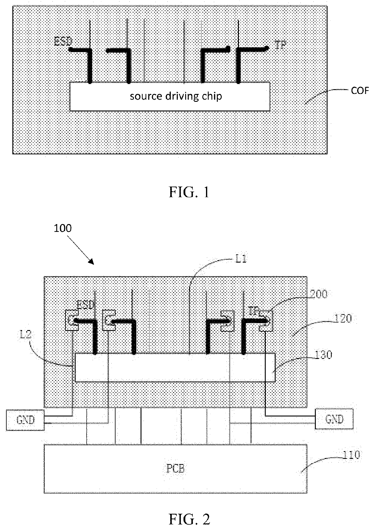
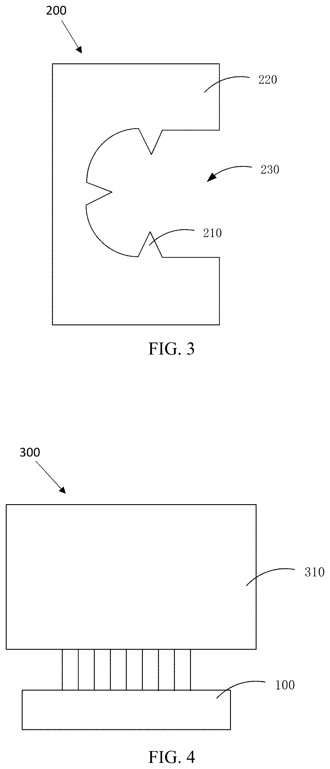
[0015]In the following, the technical solutions in the embodiments of the present disclosure will be clearly and completely described with reference to the figures. Obviously, the described embodiments are only a part of the embodiments of the present disclosure, not all the embodiments. Based on the embodiments in the present disclosure, all other embodiments obtained by a person of ordinary skill in the art without creative steps shall fall within the protection scope of the present disclosure.

[0016]Unless otherwise defined, all technical and scientific terms used herein have the same meanings as commonly understood by those skilled in the technical field of the present disclosure; the terms used in the specification of the disclosure herein are for the purpose of describing specific embodiments only, not intended to limit the present disclosure; the terms “including” and “having” and any variations thereof in the description and claims of the application and the above description...


PUM


Abstract

The present disclosure provides a source driver and a display panel. The source driver includes a printed circuit board, a flip-chip film, a source driver chip, a first connection line, and a test point. The source driver chip is encapsulated on the flip-chip film and connected to the display panel through the first connection line, and the first connection line is connected to the test point, wherein a conductive pattern is formed on the flip-chip film, the conductive pattern is grounded through a ground line, and the conductive pattern includes a tip portion configured to form a tip discharge effect to discharge static electricity on the test point to the ground line. Therefore, the present disclosure can conduct static electricity through the tip portion when electrostatic discharge occurs, thereby preventing the electrostatic discharge from damaging the driver chip through a test point path.

Description

[0001]The present disclosure relates to the field of display technologies, and more particularly, to a source driver and a display device.BACKGROUND OF INVENTION[0002]Liquid crystal displays (LCDs) have many advantages such as thin body, power saving, no radiation, etc., and have been widely used, such as in LCD TVs, mobile phones, personal digital assistants (PDAs), digital cameras, computer screens or laptop screens, etc., dominating the field of flat panel displays.[0003]Electro-static discharge (ESD) refers to a charge transfer caused by objects with different electrostatic potentials coming close to or in direct contact with each other. The electrostatic discharge will generate a transient voltage of thousands of volts, causing electrostatic damage and making liquid crystal display devices unable to operate normally. In order to prevent electrostatic damage, ESD tests need to be performed during production of liquid crystal display devices.[0004]In a current chip on flex or chi...

Claims


Application Information

Patent Timeline
IPC IPC(8): G02F1/1362H05K1/02G09G3/00
CPCG02F1/136204H05K1/0259G09G2330/04G02F1/136286G09G3/006G09G3/3685H05K1/0268G09G2300/0426
Inventor CHEN, YONGQUAN
Owner TCL CHINA STAR OPTOELECTRONICS TECH CO LTD
Why Eureka
Try Eureka