Electronic module for chip card

Pending Publication Date: 2021-12-30
SMART PACKAGING SOLUTIONS SPS
View PDF2 Cites 0 Cited by
  • Summary
  • Abstract
  • Description
  • Claims
  • Application Information

AI Technical Summary

Benefits of technology

The invention is about a new way to make an electronic module for a chip card that allows for more flexibility in the design of the antenna and reduces manufacturing costs. This is done by combining a single-sided film with a more complex piece that contains at least one electrically conductive region, like an antenna. This method ensures that the chip card can still function either as a contact or contactless card.

Problems solved by technology

The type of substrate used is generally quite expensive.

Method used


Image

  • Electronic module for chip card
  • Electronic module for chip card
  • Electronic module for chip card

Examples


Embodiment Construction

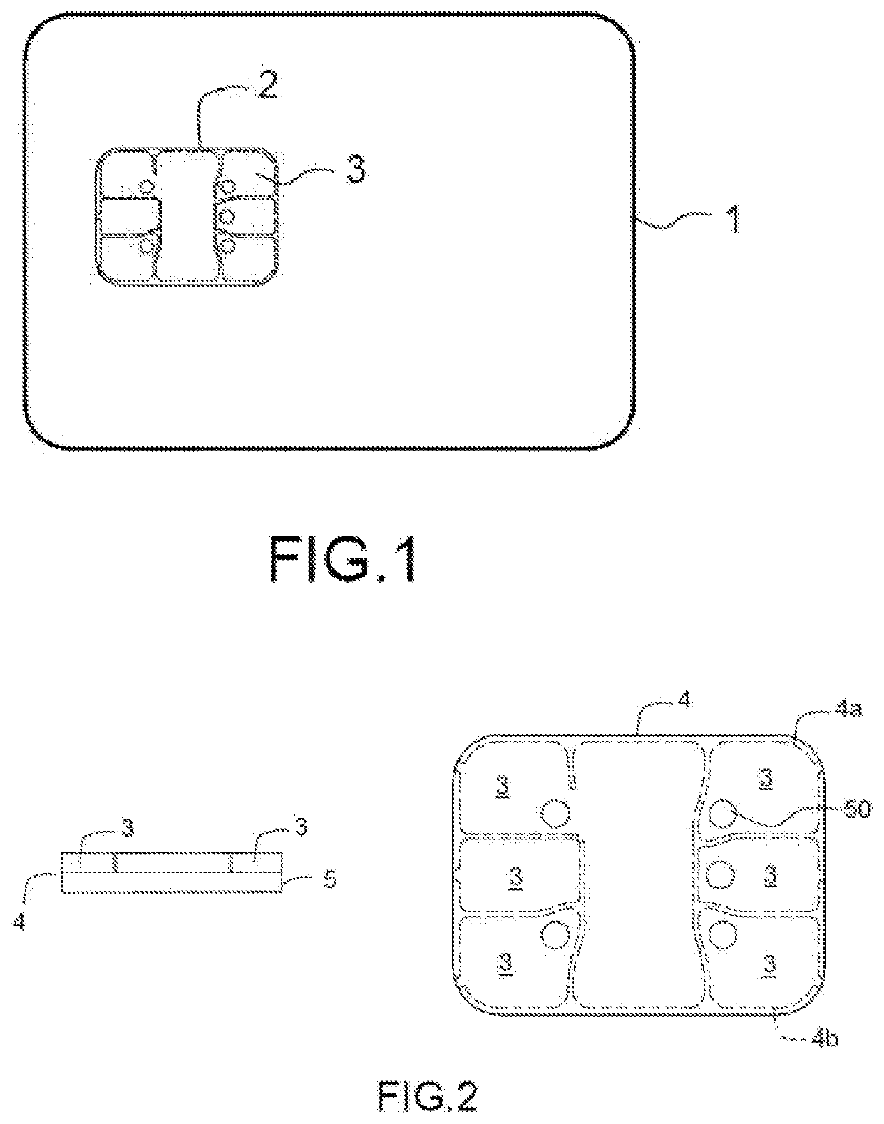
[0041]The following description is given by way of entirely non-limiting illustration for the production of a module for a dual-interface card. The steps described below may, without departing from the scope of the invention, be used for electronic modules intended for credit cards, SIM cards for mobile phones, transport cards, identity cards, etc.

[0042]For the sake of simplicity of the description, the figures show a single module, it being known that the antennas will, in most cases, be produced over a wide width (a few tens of cm to several meters), allowing higher production.

[0043]FIG. 1 illustrates a chip card 1 comprising at least one electronic module 2 obtained by implementing the process according to the invention. The electronic module 2 integrated into the chip card 1 has contacts 3 or contact regions at the level of the surface of the front face of the card in order to allow electrical connection thereof with a card reader, not shown for the sake of simplicity of the dra...


PUM


Abstract

A process for manufacturing an electronic module intended to be implemented in a dual-interface portable object is provided. The process includes at least the following steps:Using a single-sided film consisting of one or more contact regions and a dielectric comprising one or more apertures,Using a substrate comprising one or more electrically conductive regions intended for the contactless communication of the object,Securing said single-sided film and said substrate together,Positioning an integrated circuit and connecting it to the contact regions of the single-sided film and at least to one terminal of at least one of said electrically conductive regions,Depositing a protective layer incorporating at least said integrated circuit.Also provided is a module obtained by means of the process.

Description

CROSS-REFERENCE TO RELATED APPLICATIONS[0001]The present application is a national phase entry of PCT / EP2019 / 077275, filed on Oct. 9, 2019, which claims the benefit of priority of French Application No. 1860297, filed Nov. 8, 2018, the entire contents of which are hereby incorporated by reference in their entirety for all purposes.TECHNICAL FIELD[0002]The invention relates to an electronic module for a portable object having a dual, contact and contactless, function, for example a chip card.BACKGROUND[0003]Electronic modules are generally produced on flexible printed circuit boards with one or two etched and metallized copper layers. The pads of the integrated circuit chip are electrically connected to the contact plates of the connection package by means of conductive wires. In order to be able to electrically connect the electronic module to another electrical circuit embedded in the card body, the electronic module further comprises an antenna or a pair of contact plates internal...

Claims


Application Information

Patent Timeline
IPC IPC(8): G06K19/077
CPCG06K19/07754G06K19/07775G06K19/07769G06K19/07745G06K19/0775
Inventor CALVAS, BERNARDVOLPE, PIERRE
Owner SMART PACKAGING SOLUTIONS SPS
Why Eureka
Try Eureka