Integrated circuit devices with highly integrated memory and peripheral circuits therein

Pending Publication Date: 2022-01-27
SAMSUNG ELECTRONICS CO LTD
View PDF0 Cites 0 Cited by
  • Summary
  • Abstract
  • Description
  • Claims
  • Application Information

AI Technical Summary

Benefits of technology

[0004]Example embodiments of the invention provide highly integrated vertical semicon

Problems solved by technology

As a height in a vertical direction of the cell stack structure increases, a planarization process of an upper surface of the insu

Method used


Image

  • Integrated circuit devices with highly integrated memory and peripheral circuits therein
  • Integrated circuit devices with highly integrated memory and peripheral circuits therein
  • Integrated circuit devices with highly integrated memory and peripheral circuits therein

Examples


Example

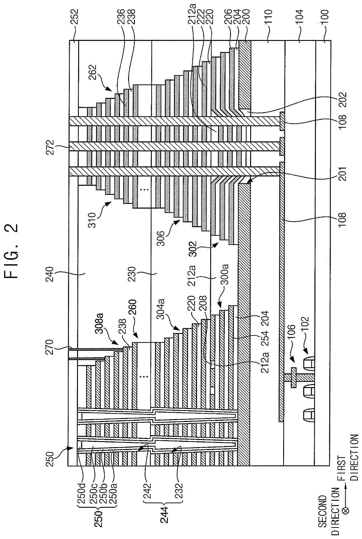
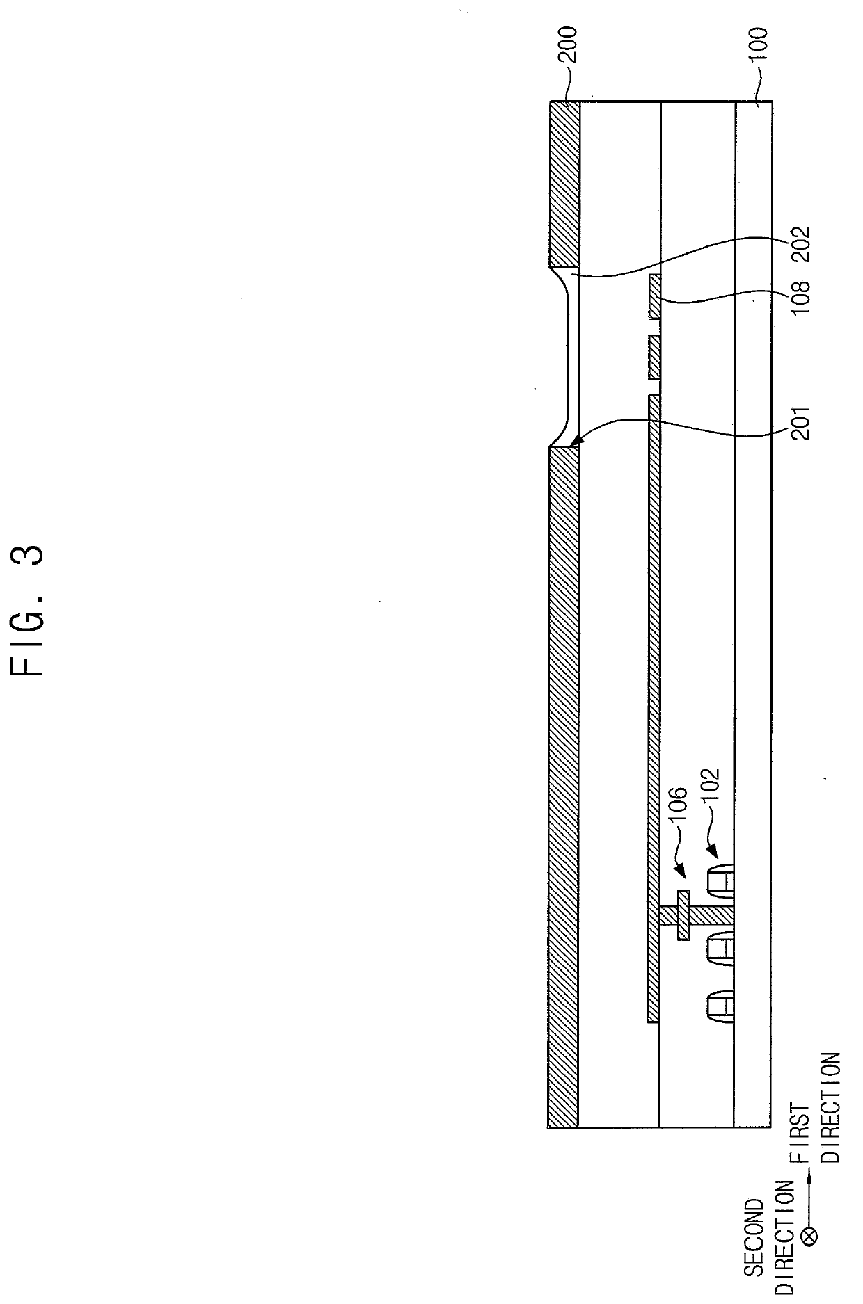
[0017]Hereinafter, a direction substantially perpendicular to an upper surface of the substrate is defined as a vertical direction, and two directions crossing with each other in horizontal directions substantially parallel to the upper surface of the substrate are defined as first and second directions, respectively. In example embodiments, the first and second directions may be perpendicular to each other.

[0018]FIG. 1 is a cross-sectional view illustrating a vertical semiconductor device in accordance with example embodiments. FIG. 2 is a cross-sectional view illustrating a vertical semiconductor device in accordance with some example embodiments. Referring to FIG. 1, the vertical semiconductor device may include circuit patterns constituting a peripheral circuit on a substrate 100. In example embodiments, the circuit pattern may include lower transistors 102 and lower wiring 106. The lower wiring 106 may include lower contact plugs and lower conductive patterns. The lower wiring ...


PUM


Abstract

An integrated circuit device includes a vertical stack of nonvolatile memory cells on a substrate, which are configured as a vertical NAND string of memory cells. This vertical stack of nonvolatile memory cells includes a plurality of gate patterns, which are spaced apart from each other by corresponding electrically insulating layers. A dummy mold structure is also provided on the substrate. The dummy mold structure includes a vertical stack of sacrificial layers, which are spaced apart from each other by corresponding electrically insulating layers. An insulation pattern is provided, which fills a dish-shaped recess in a first one of the sacrificial layers in the vertical stack of sacrificial layers. This insulation pattern has an upper surface that is coplanar with an upper surface of the first one of the sacrificial layers.

Description

REFERENCE TO PRIORITY APPLICATION[0001]This application claims priority under 35 USC § 119 to Korean Patent Application No. 10-2020-0093215, filed Jul. 27, 2020, the contents of which are hereby incorporated herein by reference.BACKGROUND1. Field[0002]Example embodiments relate to integrated circuit devices and, more particularly, to integrated circuit devices having vertically and highly integrated semiconductor devices therein and methods of forming same.2. Description of the Related Art[0003]As semiconductor devices become more highly integrated, a VNAND flash memory device may utilize a cell-on-peripheral (COP) structure in which a peripheral circuit is formed on a substrate and cell stack structures including memory cells are stacked on the peripheral circuit. An insulating interlayer may be formed between the cell stack structures. As a height in a vertical direction of the cell stack structure increases, a planarization process of an upper surface of the insulating interlayer...

Claims


Application Information

Patent Timeline
IPC IPC(8): H01L27/11573H01L23/535H01L27/11556H01L27/11529H01L27/11582
CPCH01L27/11573H01L23/535H01L27/11582H01L27/11529H01L27/11556H10B43/50H10B43/27H10B43/40H10B41/27H10B41/41
Inventor HWANG, CHANGSUNKIM, GIHWANSEOK, HANSOLLIM, JONGHEUNJANG, KISEOK
Owner SAMSUNG ELECTRONICS CO LTD
Why Eureka
Try Eureka