Electronic device for compensating for loss of inter frequency signal between antenna module and inter frequency integrated circuit

Pending Publication Date: 2022-01-27
SAMSUNG ELECTRONICS CO LTD
View PDF0 Cites 0 Cited by
  • Summary
  • Abstract
  • Description
  • Claims
  • Application Information

AI Technical Summary

Benefits of technology

The patent describes an electronic device that can compensate for signal loss between a frequency converter and a radio frequency integrated circuit, even if the distance between them increases. This is achieved through the use of multiple compensation units that can amplify the signal loss and restore it to its original form. The device also includes a foldable or unfoldable design that allows for efficient use of space and includes specific placement of the integrated circuits to minimize signal loss. Overall, the invention improves the stability and reliability of wireless communication systems.

Problems solved by technology

It is not easy for an electronic device to modulate a high-frequency RF signal into a digital signal, which is directly processed by a modem, or to modulate the digital signal into an RF signal.

Method used


Image

  • Electronic device for compensating for loss of inter frequency signal between antenna module and inter frequency integrated circuit
  • Electronic device for compensating for loss of inter frequency signal between antenna module and inter frequency integrated circuit
  • Electronic device for compensating for loss of inter frequency signal between antenna module and inter frequency integrated circuit

Examples


Embodiment Construction

[0034]Hereinafter, various example embodiments of the disclosure may be described with reference to accompanying drawings. However, those of ordinary skill in the art will recognize that modification, equivalent, and / or alternative on various embodiments described herein may be variously made without departing from the scope and spirit of the disclosure.

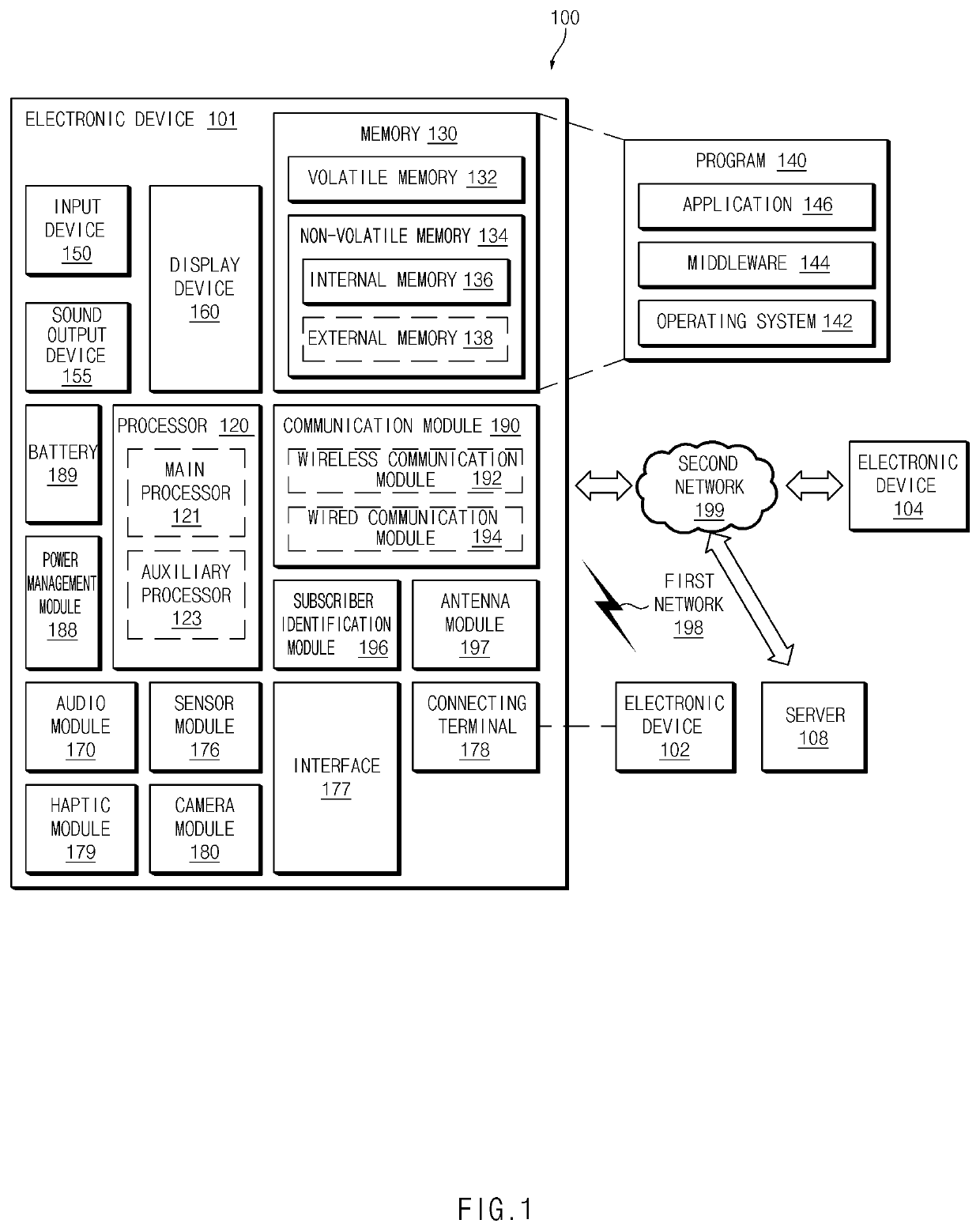
[0035]FIG. 1 is a block diagram illustrating an example electronic device 101 in a network environment 100 according to various embodiments. Referring to FIG. 1, the electronic device 101 in the network environment 100 may communicate with an electronic device 102 via a first network 198 (e.g., a short-range wireless communication network), or an electronic device 104 or a server 108 via a second network 199 (e.g., a long-range wireless communication network). According to an embodiment, the electronic device 101 may communicate with the electronic device 104 via the server 108. According to an embodiment, the electronic device 101 m...


PUM


Abstract

Disclosed is an electronic device including a plurality of radio frequency integrated circuits (RFICs) that delivers a digital signal, which is to be transmitted by a modem through an antenna configured to transmit and / or receive a radio frequency (RF) signal, in a form of the RF signal and to deliver the RF signal received from the antenna, in a direction of the modem, wherein the plurality of RFICs are at least partially connected to one another, an inter frequency integrated circuit (IFIC) connected to at least some RFICs among the plurality of RFICs and configured to receive the digital signal from the modem, to convert the digital signal to an inter frequency (IF) signal, to deliver the IF signal to the RFIC, to convert the RF signal delivered from the RFIC to the IF signal, and to deliver the IF signal to the modem, and a plurality of compensation units respectively connected to the plurality of RFICs or respectively positioned inside of the plurality of RFICs, the compensation units comprising circuitry configured to compensate for a loss of the IF signal occurring between the IFIC and the at least some RFICs or to compensate for a loss of the IF signal occurring between the plurality of RFICs.

Description

CROSS-REFERENCE TO RELATED APPLICATIONS[0001]This application is a continuation of International Application No. PCT / KR2020 / 00412 designating the United States, filed on Jan. 9, 2020, in the Korean Intellectual Property Receiving Office and claiming priority to Korean Patent Application No. 10-2019-0039879, filed on Apr. 5, 2019, in the Korean Intellectual Property Office, the disclosures of which are incorporated by reference herein in their entireties.BACKGROUNDField[0002]The disclosure relates to a technology for implementing an electronic device that compensates for the loss of an inter frequency signal between an antenna module and an inter frequency integrated circuit.Description of Related Art[0003]As mobile communication technologies develop, an electronic device equipped with an antenna is being widely supplied. The electronic device may transmit and / or receive a radio frequency (hereinafter referred to as ‘RF’) signal including a voice signal or data (e.g., a message, a ph...

Claims


Application Information

Patent Timeline
IPC IPC(8): H01Q1/22H01Q9/04H01Q21/00
CPCH01Q1/2283H01Q21/0075H01Q9/0457H04B1/12H04B1/401H04M1/02H04B1/40H04B1/00H01Q1/243H01Q21/28H01Q3/34H04B1/0064H04M1/026
Inventor HONG, SUKCHANDO, MINHONGPARK, SEONGJINLEE, KYUNGROKLEE, SEOKWOOCHUN, JAEBONGCHOI, HYUNSUK
Owner SAMSUNG ELECTRONICS CO LTD
Why Eureka
Try Eureka