Electronic device for converting a wireless signal into at least one modulated optical signal

a wireless signal and optical signal technology, applied in the field of electronic devices for converting wireless signals into modulated optical signals, can solve the problems of low conversion loss, low frequency performance, and high cost of iii-v technologies, and achieve the effect of broad frequency performance and low conversion loss

Active Publication Date: 2022-02-17
ETH ZZURICH
View PDF6 Cites 0 Cited by
  • Summary
  • Abstract
  • Description
  • Claims
  • Application Information

AI Technical Summary

Benefits of technology

[0009]There may be a need for an improved electronic device for converting a wireless signal into at least one modulated optical signal. More particularly, there may be a need for a compact, inexpensive electronic device for converting a wireless signal in the mm wave or sub-THz range into at least one modulated optical signal. More particularly, there may be a need for an electronic device for converting a wireless signal in the mm wave or sub-THz range into at least one modulated optical signal having low conversion loss and broad frequency performance.

Problems solved by technology

In the prior art, employed are expensive III-V technologies, relying on a high cost substrates and a limited maximum wafer size, discrete components and antennas, which have disadvantages as regards compactness, cost, conversion loss and frequency range.
However the conversion is strongly limited in terms of high loss; in terms of speed by the bandwidth of the modulator; the low nonlinear coefficient requires a large structure (cm-scale), therefore with high bulk and fabrication cost.
“Direct conversion of free space millimeter waves to optical domain by plasmonic modulator antenna.” Nano letters 15.12 (2015): 8342-8346, discloses a compact structure operating at high frequency (60 GHz); however the structure does not allow high conversion efficiency.

Method used


Image

  • Electronic device for converting a wireless signal into at least one modulated optical signal
  • Electronic device for converting a wireless signal into at least one modulated optical signal
  • Electronic device for converting a wireless signal into at least one modulated optical signal

Examples


first embodiment

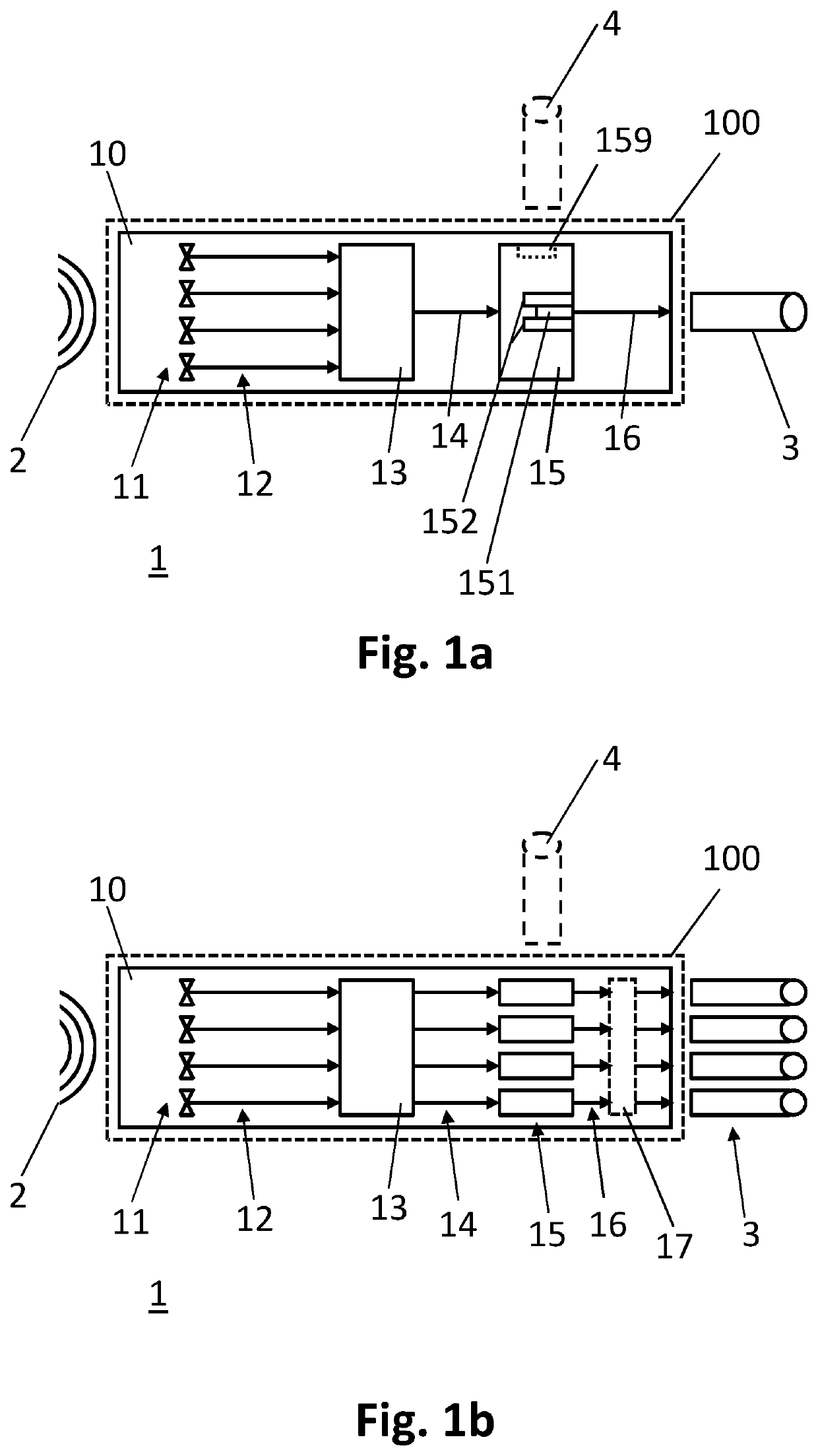
[0042]FIG. 1a shows an electronic device 1 for converting a wireless signal in the mm-wave or sub-THz range into at least one modulated optical signal. The electronic device 1 receives a wireless signal 2 and converts the wireless signal into at least one modulated optical signal 16, which can be transmitted by at least one optical fibre 3. FIG. 1a illustrates the case of one modulated optical signal 16 and one optical fibre 3. The wireless signal 2 is in the mm-wave or sub-THz range. According to the embodiment illustrated in FIG. 1a, at least one antenna elements 11, an electrical signal converter 13 and at least one modulator 15 are arranged on a single integrated chip 10. The at least one modulator 15 according to FIG. 1a includes one modulator. As illustrated in FIG. 1a, the single integrated chip 10 may be enclosed in a microchip package 100. The at least one antenna element 11 may include a number N of antenna elements. The at least one antenna element 11 may comprise one, tw...

second embodiment

[0043]FIG. 1b schematically shows an electronic device 1 for converting a wireless signal in the mm-wave or sub-THz range into at least one modulated optical signal 16. The electronic device 1 includes at least one antenna element 11, an electric signal converter 13, and at least one modulator 15 having the functions as described above in connection with FIG. 1a. As illustrated in FIG. 1b, the at least one antenna element 11 respectively the at least one guided electrical signal 12 include a number N=4 antenna elements respectively guided electrical signals. As illustrated in FIG. 1b, the at least one guided electrical signal 12 respectively the at least one modulator 15 includes a number M=4 guided electrical signals respectively modulators. In some embodiments of the electronic device 1, the number N may be two, four, eight, sixteen or any other number. In some embodiments of the electronic device the number M may be two, four, eight, sixteen or any other number.

[0044]As illustrat...

fourth embodiment

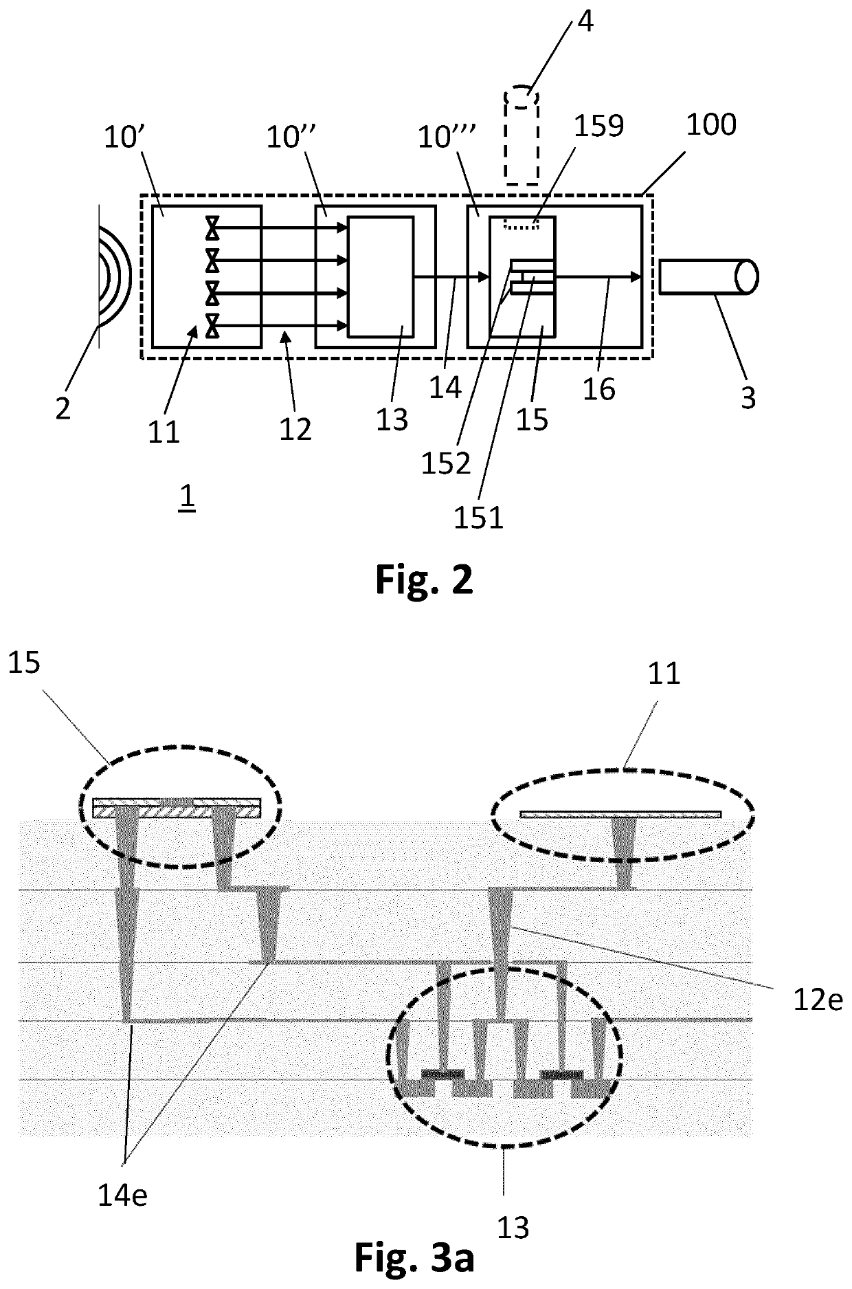
[0046]In a fourth embodiment, which is not illustrated in FIG. 1a or FIG. 1b or FIG. 2, the at least one antenna element 11 and the electrical signal convertor 13 may be arranged on a single integrated chip, and the at least one modulator 15 may be arranged on another single integrated chip.


PUM


Abstract

Disclosed is an electronic device (1) for converting a wireless signal (2) in the mm-wave or sub-THz range into at least one modulated optical signal (16). The electronic device (1) comprises an antenna element (11) for converting the wireless signal (2) into a guided electrical signal (12), wherein the antenna element (11) is arranged on a printed circuit board (10b′) or on a first integrated chip (10′)′ The electronic device (1) comprises an electrical signal converter (13) for converting the at least one guided electrical signal (12) into a conditioned electrical signal (14), wherein the electrical signal converter (13) is arranged on a second integrated chip (10″). The electronic device (1) comprises a modulator (15) for converting the conditioned electrical signal (14) into the modulated optical signal (16), wherein the modulator (15) is arranged on a third integrated chip (10′″), and wherein the modulator (15) comprises a waveguide (151) and a cladding (152) comprising a first cladding portion (1521) having a conductive material at an interface with the waveguide (151) and a second cladding portion (1522) having a conductive material at an interface with the waveguide (151).

Description

FIELD OF THE INVENTION[0001]The present disclosure relates to an electronic device for converting a wireless signal into at least one modulated optical signal. More particularly, the present disclosure relates to an electronic device for converting a wireless signal in the mm wave or sub-THz range into at least one modulated optical signal.BACKGROUND ART[0002]Conversion of a wireless signal into at least one modulated optical signal is required in many applications. A wireless signal in the range from 30 MHz-30 GHz belongs to the class of microwaves. A wireless signal in the range from 30 GHz-300 GHz belongs to the class of millimetre waves respectively mm waves. A wireless signal in the range from 300 GHz-1 THz belongs to the class of sub-THz waves respectively to the sub-THz range.[0003]The receiver may convert the wireless signal into an electrical signal and convert the electrical signal into at least one modulated optical signal. Ideally, a broad frequency range may be covered ...

Claims


Application Information

Patent Timeline
Patent Type & Authority Applications(United States)
IPC IPC(8): H04B10/2575H04B10/80
CPCH04B10/25759H04B10/801H04B10/25751H04B10/2575
Inventor BURLA, MAURIZIOLEUTHOLD, JUERG
Owner ETH ZZURICH
Why Eureka
Try Eureka