

Method and Apparatus for Detecting Positions of Wafers
- Summary
- Abstract
- Description
- Claims
- Application Information
AI Technical Summary
Benefits of technology
Problems solved by technology
Method used
Image

Examples
Embodiment Construction
[0030]In the following detailed description, many specific details are explained in order to provide a thorough understanding of the present invention. However, those of ordinary skill in the art will understand that the present invention can be practiced without these specific details. In other cases, well-known methods, procedures and / or elements have not been described in detail so as not to obscure the present invention.
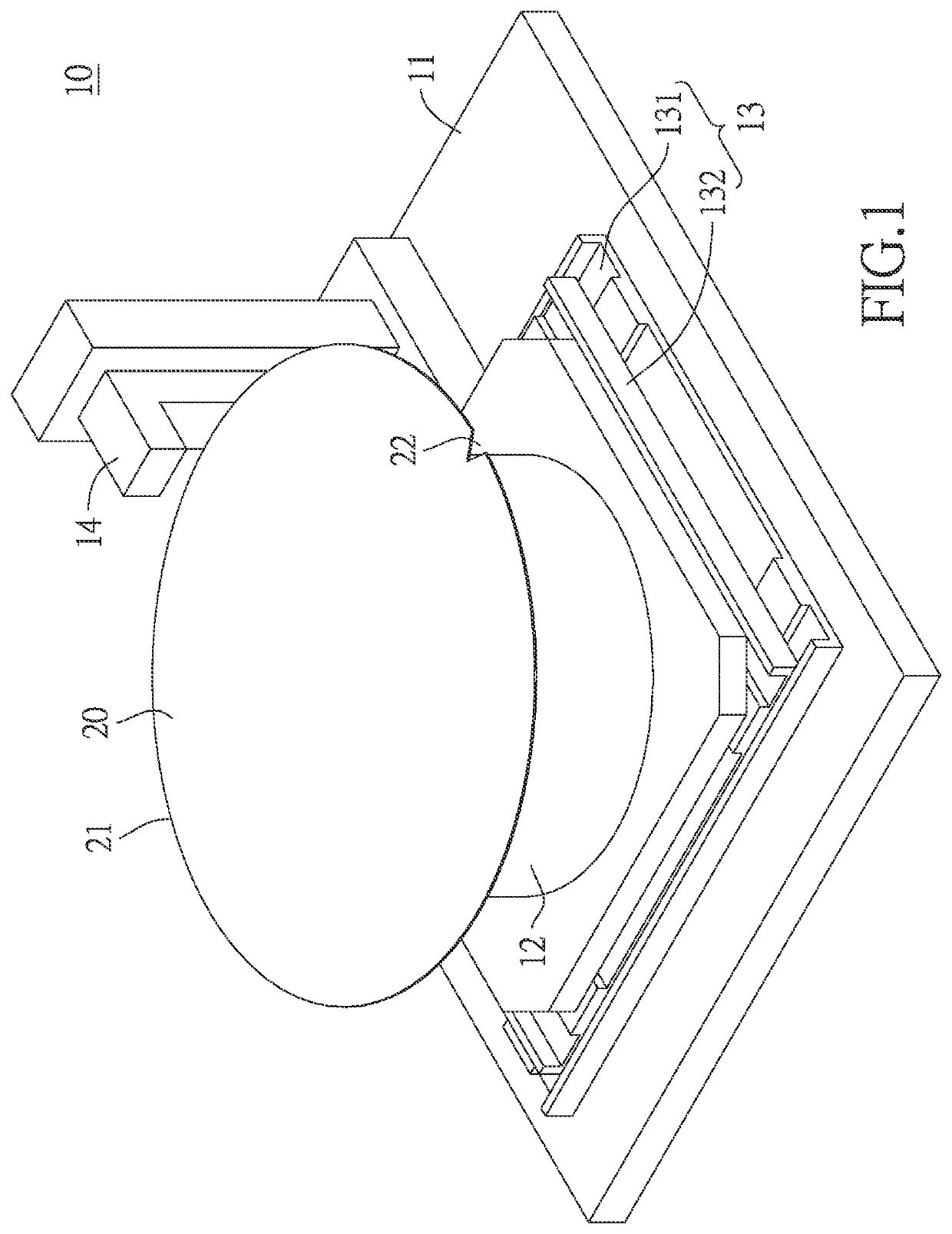
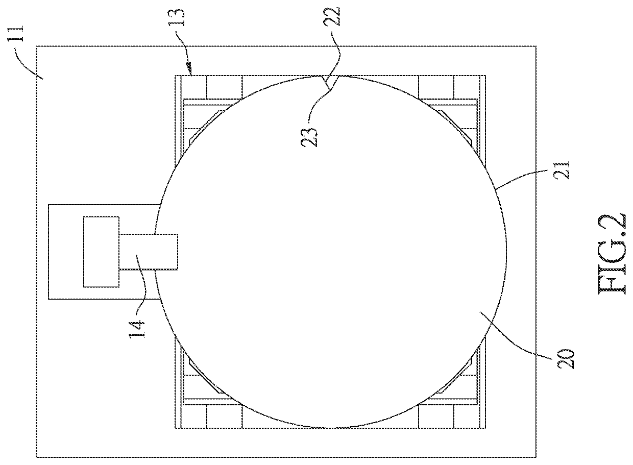
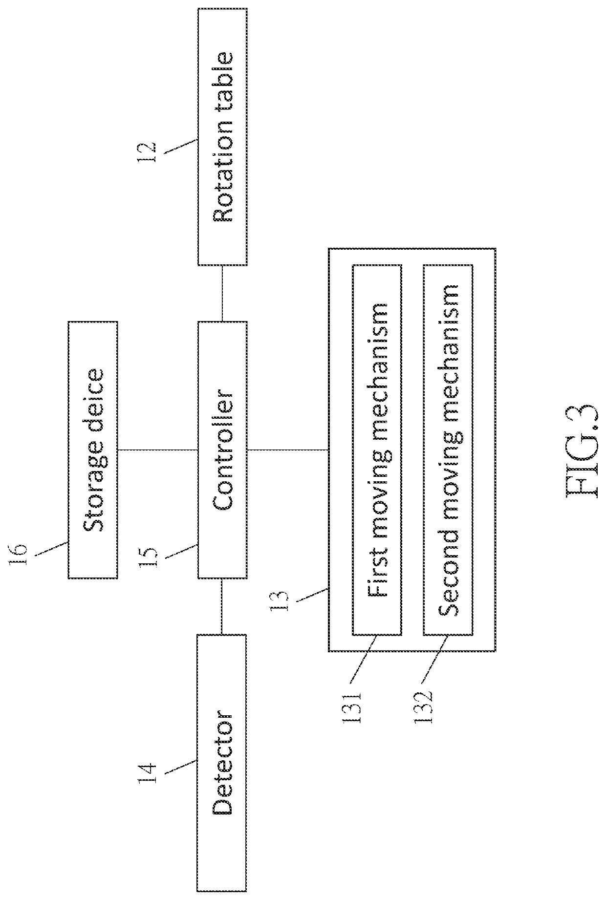
[0031]Please refer to FIGS. 1 to 3, a system 10 for detecting positions of wafers according to an embodiment of the present invention is adapted to be applied to a wafer aligner (i.e., an apparatus capable of detecting positions of wafers and aligning and correcting the positions of the wafers), and the system 10 for detecting positions of wafers includes a base 11, a rotation table 12, a moving platform 13, a detector 14, a controller 15 and a storage device 16. The rotation table 12, the moving platform 13 and the detector 14 are arranged to the base 11, and th...
PUM
 Abstract
Description
Claims
Application Information