Semiconductor device

a technology of semiconductors and semiconductor parts, applied in the direction of individual semiconductor device testing, heat measurement, instruments, etc., can solve the problems of semiconductor destruction, and achieve the effect of accurately detecting the temperature of the transistor part and the temperature, and improving the function of overheat protection

Active Publication Date: 2022-03-03
MITSUBISHI ELECTRIC CORP
View PDF7 Cites 0 Cited by
  • Summary
  • Abstract
  • Description
  • Claims
  • Application Information

AI Technical Summary

Benefits of technology

[0004]However, the conventional technique can detect the temperature of the whole semiconductor chip accurately, but has one temperature detection part, thus cannot follow a rapid increase in temperature of each of the transistor part and the diode part, so that it has a problem that a thermal destruction of the semiconductor chip occurs before the temperature detection part detects an overheat of the transistor part and the diode part.
[0005]An object of the present disclosure is to provide a semiconductor device capable of accurately detecting a temperature of a transistor part and a temperature of the diode part, and improving an overheat protection function.

Problems solved by technology

However, the conventional technique can detect the temperature of the whole semiconductor chip accurately, but has one temperature detection part, thus cannot follow a rapid increase in temperature of each of the transistor part and the diode part, so that it has a problem that a thermal destruction of the semiconductor chip occurs before the temperature detection part detects an overheat of the transistor part and the diode part.

Method used


Image

  • Semiconductor device
  • Semiconductor device
  • Semiconductor device

Examples


embodiment 1

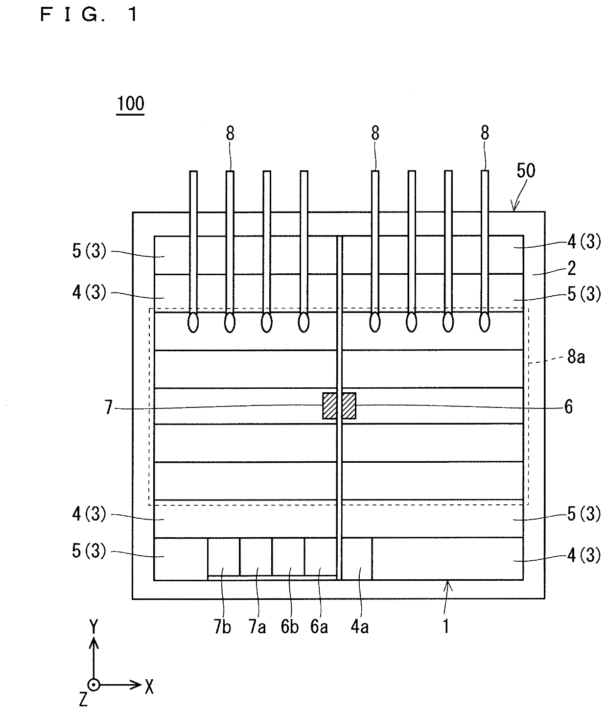
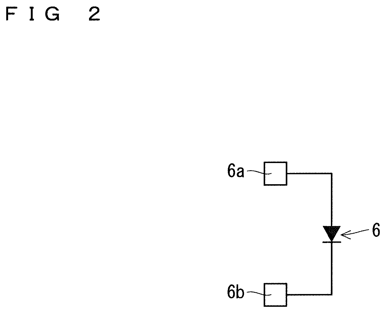
[0018]An embodiment 1 is described hereinafter using the drawings. FIG. 1 is a pattern diagram of a structure of an upper surface of a semiconductor device 100 according to the embodiment 1. FIG. 2 is a circuit diagram of a temperature detection part 6. XYZ coordinate axes are appropriately illustrated in the drawings to simplify the description. Herein, a +X direction and a −X direction are collectively referred to as an X-axis direction, a +Y direction and −Y direction are collectively referred to as a Y-axis direction, and a +Z direction and −Z direction are collectively referred to as a Z-axis direction.

[0019]As illustrated in FIG. 1, a semiconductor device 100 includes a semiconductor chip 50, a temperature detection part 6 as a first temperature detection part, a temperature detection part 7 as a second temperature detection part, and an external wiring 8. The semiconductor device 100 further includes an insulating layer made up of ceramic or resin, a metal pattern formed on t...

embodiment 2

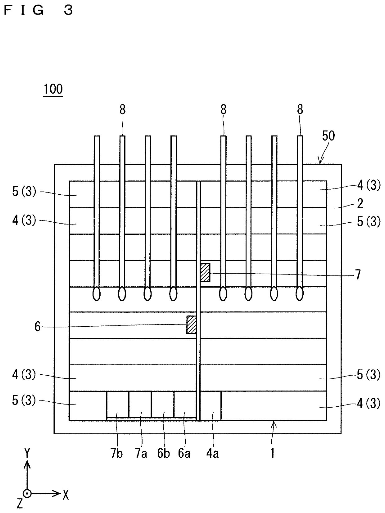
[0033]Next, a semiconductor device 100 according to an embodiment 2 is described. FIG. 3 is a pattern diagram of a structure of an upper surface of the semiconductor device 100 according to the embodiment 2. FIG. 4 is a pattern diagram of a structure of an upper surface in another example of the semiconductor device 100 according to the embodiment 2. In the embodiment 2, the same reference numerals are assigned to the same constituent elements described in the embodiment 1, and the description thereof will be omitted.

[0034]As illustrated in FIG. 3 and FIG. 4, in the embodiment 2, one end portion of each of the plurality of external wirings 8 is connected to the cell 3 adjacent to the cells 3 where the temperature detection part 6 and the temperature detection part 7 are disposed, respectively. One end portion of each of the plurality of external wirings 8 is connected to a position close to the temperature detection part 6 and the temperature detection part 7 compared with the case ...

embodiment 3

[0037]Next, a semiconductor device 100 according to an embodiment 3 is described. FIG. 5 is a pattern diagram of a structure of an upper surface of the semiconductor device 100 according to the embodiment 3. In the embodiment 3, the same reference numerals are assigned to the same constituent elements described in the embodiments 1 and 2, and the description thereof will be omitted.

[0038]As illustrated in FIG. 5, in the embodiment 3, the connection by the external wiring 8 is a stitch connection connected to the cell region 1 at a plurality of positions. The stitch connection indicates a connection method of connecting each external wiring 8 and the semiconductor chip 50 at a plurality of positions. When there is no stitch connection, each external wiring 8 and the semiconductor chip 50 are connected at one position. In contrast, when there is a stitch connection, each external wiring 8 and the semiconductor chip 50 are connected at two positions. The number of positions at which ea...


PUM

PropertyMeasurementUnit
temperatureaaaaaaaaaa
protection threshold valueaaaaaaaaaa
temperature detectionaaaaaaaaaa

Abstract

An object is to provide a semiconductor device capable of accurately detecting a temperature of a transistor part and a temperature of the diode part, and improving an overheat protection function. A semiconductor device includes a semiconductor chip having a cell region made up of a plurality of cells including cells corresponding to a transistor part and a diode part, respectively, a temperature detection part detecting a temperature of the transistor part, and a temperature detection part detecting a temperature of the diode part, the temperature detection part is disposed in the cell corresponding to the transistor part, and the temperature detection part is disposed in the cell corresponding to the diode part.

Description

BACKGROUND OF THE INVENTIONField of the Invention[0001]The present disclosure relates to a semiconductor device including a semiconductor chip and a temperature detection part.Description of the Background Art[0002]There is conventionally a semiconductor device including a semiconductor chip having a cell region made up of a plurality of cells including cells corresponding to a transistor part and a diode part, respectively, and a temperature detection part detecting a temperature of the semiconductor chip. Known is a semiconductor device in which one end portion of an external wiring is connected to a cell around a temperature detection part, thus a temperature of a semiconductor chip can be appropriately detected (for example, refer to Japanese Patent Application Laid-Open No. 2019-186510).SUMMARY[0003]Recently, the semiconductor device is often used for an application with a load on one of the transistor part and the diode part. A temperature of a portion of the transistor part a...

Claims


Application Information

Patent Timeline
Patent Type & Authority Applications(United States)
IPC IPC(8): G01R31/26G01K7/01
CPCG01R31/2628G01K7/01G01R31/2632H01L23/34G01R31/3274H01L2224/49111H01L2224/49175H01L2224/4846H01L2224/0603
Inventor HIDAKA, HIROKIEGUCHI, KEISUKEAOKI, NOBUCHIKAYONEYAMA, REI
Owner MITSUBISHI ELECTRIC CORP
Why Eureka
Try Eureka