Method of ITO layout to make IC bear the high-volt electrostatic discharge

a technology of electrostatic discharge and layout, which is applied in the direction of identification means, semiconductor/solid-state device details, instruments, etc., can solve the problems of high cost, extraordinary screen action of mobile phones, and relatively complicated process, so as to improve the protection function of esd, and increase the lcd module assembly

Inactive Publication Date: 2005-12-27
WINTEK CORP
View PDF11 Cites 1 Cited by
  • Summary
  • Abstract
  • Description
  • Claims
  • Application Information

AI Technical Summary

Benefits of technology

[0007]The object of the present invention is to provide a method of ITO layout to make IC bear the high-volt electro static discharge. The major steps of a method of ITO layout to make IC bear the high-volt electro static discharge which is provided by the present invention, include: designing the suitable circuit impedance and Layout at the position of Driver IC bonding and Interface on LCD Module (COG type) in accordance with the function and use of each pin; improving the protection function of ESD (Electro Static Discharge) in increasing the LCD Module assembly on the product of the client.
[0008]The major steps of a method of ITO layout to make IC bear the high-volt electro static discharge, which can reach the above objects of the invention, include: designing the suitable circuit impedance and Layout at the position of Driver IC bonding and Interface on LCD Module (COG type) in accordance with the function and use of each pin; improving the protection function of ESD (Electro Static Discharge) in increasing the LCD Module assembly on the product of the client; wherein: connecting the pins of all VDD or VSS at the bottom of the IC and the width of ITO layout spreading over the bottom of IC after connecting VSS or VDD without influencing the layout of other pins. Discharge the static electricity that enters the position of Module Interface and dissipate the static electricity by means of the ITO layout design of the big area to improve the protection ability of IC for the electro static discharge. Serial connect an extremely high impedance (3K˜50KΩ) in the Reset Pin. Increase the impedance (100˜1000 Ω) of ITO circuit of Date bus, such as CS1.D / C,WR,RD,D0˜D7,C86 etc.

Problems solved by technology

But, due to the conventional design of ITO layout in LCD MODULE, it is necessary to greatly improve LCD MODULE(COG type) for the high-volt electro static discharge, which is on account of the drawback that LCD MODULE's unable to bear the high-volt electro static discharge causes the action of the screen on the mobile phone extraordinary.
Although one of the solutions is to add capacitors or antistatic elements on the glass, in addition to the limited applicable space, the fairly complicated process and the high cost are also the drawbacks.

Method used


Image

  • Method of ITO layout to make IC bear the high-volt electrostatic discharge
  • Method of ITO layout to make IC bear the high-volt electrostatic discharge
  • Method of ITO layout to make IC bear the high-volt electrostatic discharge

Examples


Embodiment Construction

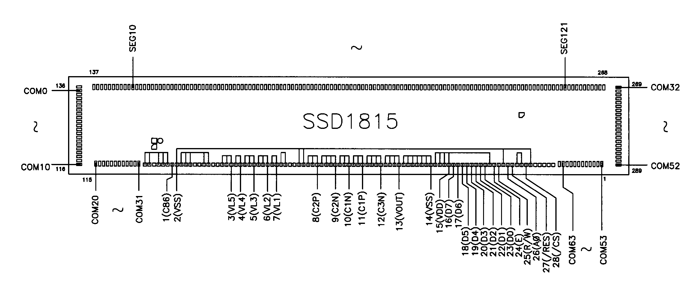
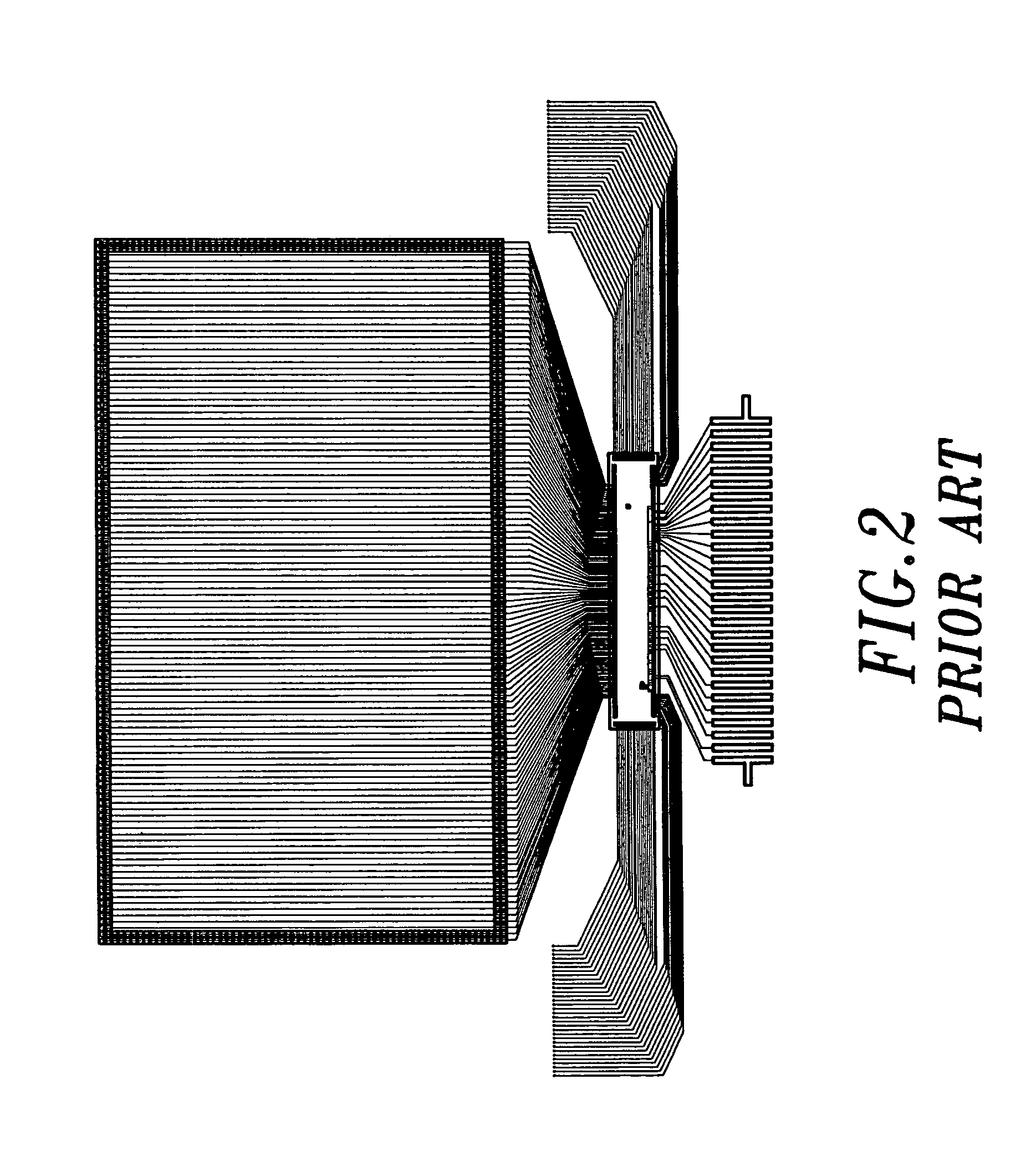
[0013]Please refer to FIG. 3. The major steps of a method of ITO layout to make IC bear the high-volt electro static discharge which is provided by the present invention, include:[0014]1. designing the suitable circuit impedance and Layout at the position of Driver IC bonding and Interface on LCD Module (COG type) in accordance with the function and use of each pin; improving the protection function of ESD (Electro Static Discharge) in increasing the LCD Module assembly on the product of the client; wherein:[0015]2. connecting the pins of all VDD or VSS together at the bottom of the IC and the width of ITO layout spreading over the bottom of IC after connecting VSS or VDD without influencing the layout of other pins;[0016]Discharging the static electricity that enters the position of Module Interface and dissipating the static electricity by means of the ITO layout design of the big area to improve the protection ability of IC for the electro static discharge;[0017]3. serial connect...


PUM

PropertyMeasurementUnit
impedanceaaaaaaaaaa
impedanceaaaaaaaaaa
impedanceaaaaaaaaaa

Abstract

The present invention provides a method of ITO layout to make IC bear the high-volt electro static discharge, wherein the major steps include: designing the suitable circuit impedance and Layout at the position of Driver IC bonding and Interface on LCD Module(COG type) in accordance with the function and use of each pin; improving the protection function of ESD(Electro Static Discharge) in increasing the LCD Module assembly on the product of the client; wherein: connecting the pins of all VDD or VSS together at the bottom of the IC and the width of ITO layout spreading over the bottom of IC without influencing the layout of other pins after connecting VSS or VDD. Discharge the static electricity that enters the position of Module Interface and dissipate the electro static discharge by means of the ITO layout design of the big area to improve the protection ability of IC for the electro static discharge. Serial connect an extremely high impedance(3K˜50K Ω) in the Reset Pin. Increase the value (100˜1000 Ω) of ITO circuit impedance of Date bus, such as CS1.D/C,WR,RD,D0˜D7,C86 etc.

Description

BACKGROUND OF THE INVENTION[0001]1. Field of the Technique[0002]The present invention relates to a method of ITO layout to make IC bear the high-volt electro static discharge.[0003]2. Description of the Prior Art[0004]It is believed that how to use the most simple way to take the shortest time to deliver all kinds of information to the consumers in the era full of information will be paid attention by the consumers, such as the quotation on the stock market or the newest information of consumption available at any time and in any place etc., and the mobile phones, the electronic mechanisms having display screen, are the best medium for the industrial and commercial world to make use in the situation that the utility rates of the mobile phones almost reach the level of everyone having a mobile phone; however, those who are skilled in this art know that the major reason why the display screen of the mobile phone can show all kinds of information is the combination of an IC connecting ...

Claims


Application Information

Patent Timeline
Patent Type & Authority Patents(United States)
IPC IPC(8): G02F1/1345G06F9/45G06F17/50G09F9/00G09F9/30G09F9/35H01L21/60H01L23/12
CPCG06F17/5036G06F17/5068H01L2924/0002H01L2924/00G06F30/367G06F30/39
Inventor WANG, HSING-FALIN, MING-CHUAN
Owner WINTEK CORP
Why Eureka
Try Eureka