Circuit board structure and manufacturing method thereof
- Summary
- Abstract
- Description
- Claims
- Application Information
AI Technical Summary
Benefits of technology
Problems solved by technology
Method used
Image
Examples
Embodiment Construction
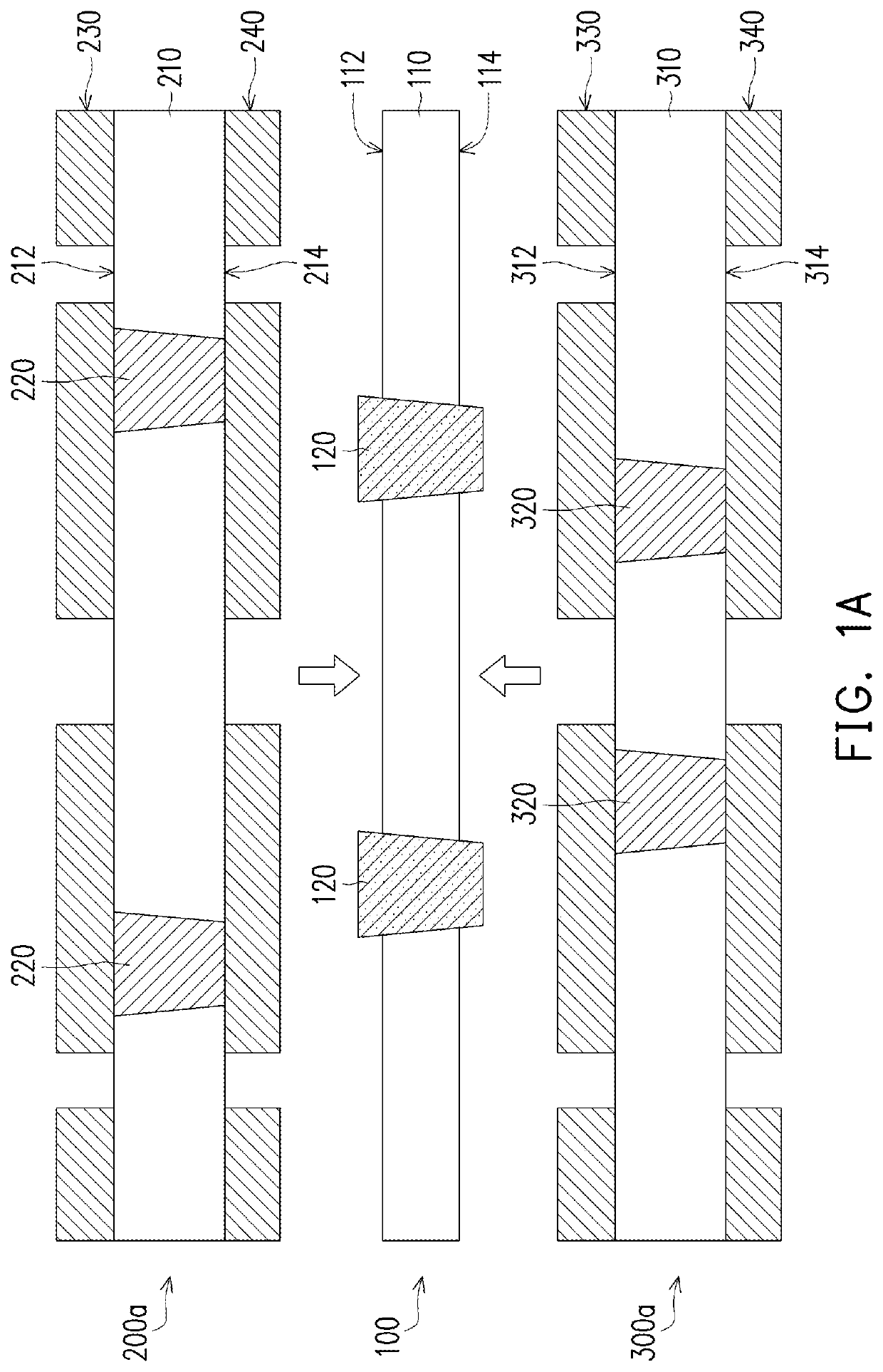
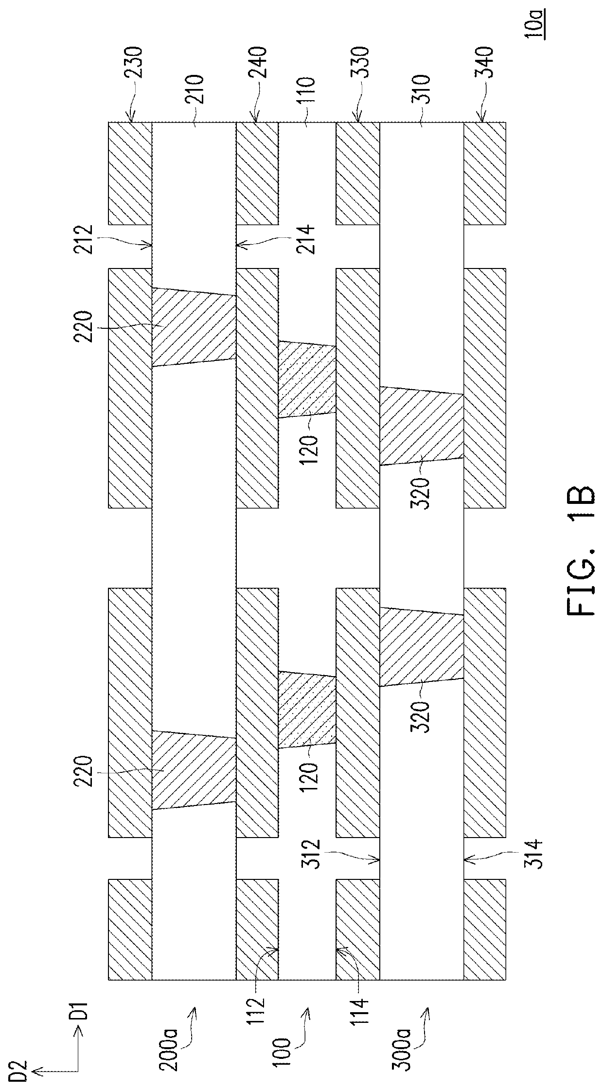
[0044]FIG. 1A to FIG. 1B are schematic cross-sectional views of a manufacturing method of a circuit board structure according to an embodiment of the invention. Regarding the manufacturing method of the circuit board structure of the present embodiment, first, referring to FIG. 1A, a first sub-circuit board 100 is provided. In detail, the first sub-circuit board 100 includes a substrate 110 and at least one first conductive through hole (two first conductive through holes 120 are schematically shown). The substrate 110 has an upper surface 112 and a lower surface 114 opposite to each other. The first conductive through holes 120 penetrate the substrate 110 and are protruded beyond the upper surface 112 and the lower surface 114. At this time, the substrate 110 is in a B-stage state, that is, the substrate 110 is in an incompletely cured state. Here, the material of the substrate 110 includes polypropylene (PP), and the material of the first conductive through holes 120 is, for examp...
PUM
 Abstract
Description
Claims
Application Information


