Solid-state imaging device

a solid-state imaging and imaging device technology, applied in semiconductor devices, radio-controlled devices, electrical devices, etc., can solve the problem of parasitic light sensitivity noise that cannot be removed, and achieve the effect of high image quality, parasitic light sensitivity noise removal, and high sensitivity

Pending Publication Date: 2022-06-02
SHARP SEMICON INNOVATION CORP
View PDF5 Cites 0 Cited by
  • Summary
  • Abstract
  • Description
  • Claims
  • Application Information

AI Technical Summary

Benefits of technology

[0005]An object of the present disclosure is to provide a solid-state imagine device that can display an image having high image quality with high sensitivity, with the parasitic light sensitivity noise removed.
[0007]The solid-state imaging device according to one aspect of the present disclosure can display an image having high image quality with high sensitivity, with parasitic light sensitivity noise removed.

Problems solved by technology

However, the solid-state imaging device according to WO 2017 / 131009 pamphlet has a problem in that parasitic light sensitivity noise cannot be removed, the noise being generated in a case where the incident light refracted toward the light reception portion is diffracted by a light blocking film to enter a memory portion.

Method used


Image

  • Solid-state imaging device
  • Solid-state imaging device
  • Solid-state imaging device

Examples


first embodiment

[0027]Hereinafter, one embodiment of the present disclosure will be described in detail.

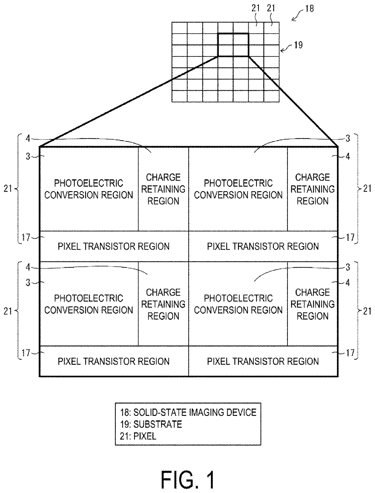
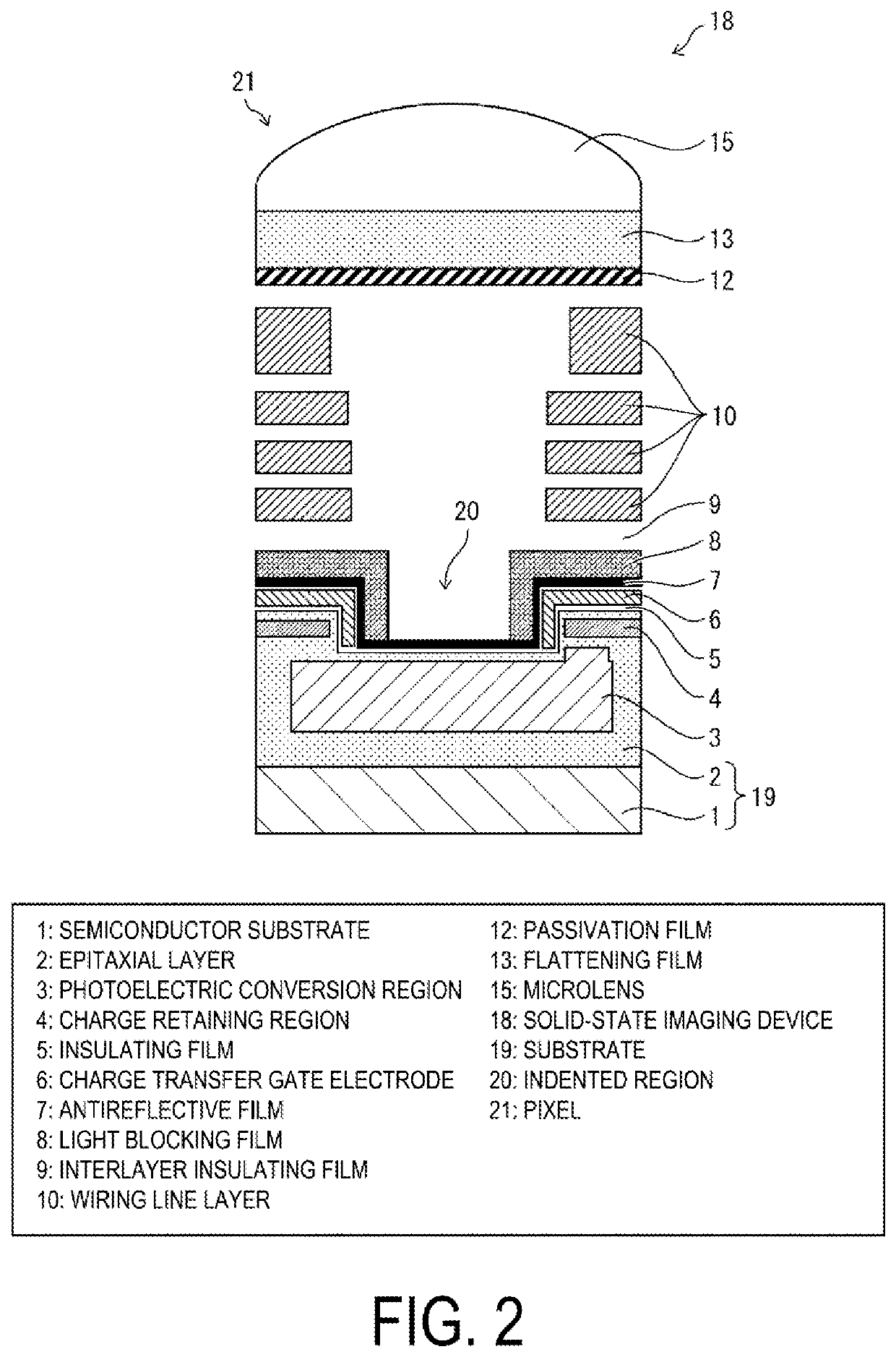
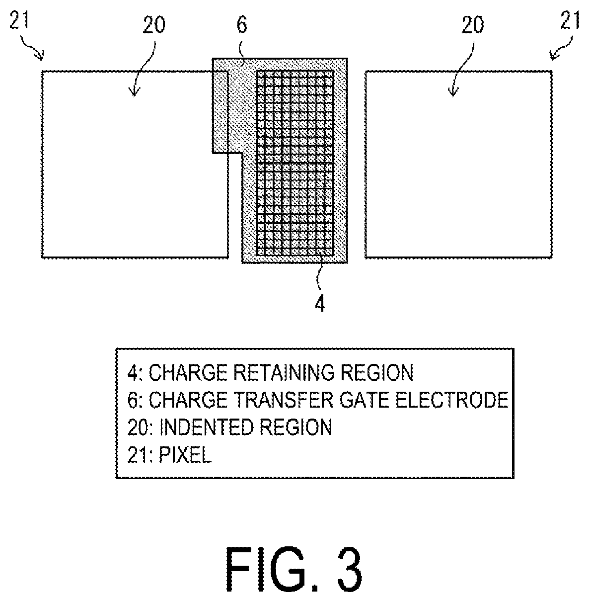
[0028]FIG. 1 is a diagram illustrating a configuration of pixels 21 arranged in a solid-state imaging device 18 according to a first embodiment. FIG. 2 is a structural cross-sectional view of a pixel 21 of the solid-state imaging device 18 according to the first embodiment. FIG. 3 is a plan view of the pixels 21.

[0029]The solid-state imaging device 18 includes a substrate 19. The substrate 19 includes a semiconductor substrate 1 and an epitaxial layer 2 formed on the semiconductor substrate 1.

[0030]The solid-state imaging device 18 includes the plurality of pixels 21 arranged in a matrix form on the substrate 19. Each pixel 21 includes: a photoelectric conversion region 3 for converting light that has entered the substrate 19 into charge; a charge retaining region 4 for retaining the charge as a result of the conversion by the photoelectric conversion region 3; and a pixel transistor region 17 in...

first modified example of first embodiment

[0076]FIG. 8 is a structural cross-sectional view of a pixel 21 of a solid-state imaging device 18A according to a first modified example of the first embodiment.

[0077]A difference from the solid-state imaging device 18 of the first embodiment is that the optical waveguide 11 is disposed between the passivation film 12 and the flattening film 13. Other structures and operations / effects are the same as those of the solid-state imaging device 18 of the first embodiment, and thus descriptions thereof will be omitted.

[0078]With the optical waveguide 11 disposed in the solid-state imaging device 18A, light that has entered the microlens 15 passes through the flattening film 13 to enter the optical waveguide 11. In the optical waveguide 11, the incident light is condensed to the center axis in a direction perpendicular to the substrate 19. The condensed incident light is emitted from the optical waveguide 11, and passes through the interlayer insulating film 9 to enter the photoelectric c...

second modified example of first embodiment

[0083]FIG. 9 is a structural cross-sectional view of a pixel 21 of a solid-state imaging device 18B according to a second modified example of the first embodiment.

[0084]A difference from the solid-state imaging device 18 of the first embodiment is that the color filter 14 is disposed between the flattening film 13 and the microlens 15. Other structures and operations / effects are the same as those of the solid-state imaging device 18 of the first embodiment, and thus descriptions thereof will be omitted.

[0085]With the color filter 14 disposed in the solid-state imaging device 18B, light of a predetermined wavelength that has entered the microlens 15 passes through the color filter 14, and light of the other wavelengths is absorbed by the color filter 14. Thus, only the light of the predetermined wavelength enters the photoelectric conversion region 3 to be subjected to the photoelectric conversion.

[0086]In the solid-state imaging device 18B of the present embodiment, the color filter...


PUM

PropertyMeasurementUnit
distanceaaaaaaaaaa
depthaaaaaaaaaa
chargeaaaaaaaaaa

Abstract

A solid-state imaging device includes: a plurality of pixels arranged in a matrix form on a substrate, wherein the plurality of pixels each include a photoelectric conversion region disposed inside the substrate and configured to convert light entering the substrate into charge, a charge retaining region disposed more on a side from which the light enters, than the photoelectric conversion region inside the substrate and configured to retain the charge converted in the photoelectric conversion region, an indented region indented from a surface of the substrate on the side from which the light enters, toward the photoelectric conversion region to at least a depth corresponding to the charge retaining region, and a light blocking film formed covering the charge retaining region at the surface side of the substrate and extending along a side wall of the indented region.

Description

CROSS-REFERENCE TO RELATED APPLICATION[0001]The present application claims priority from Japanese Application JP2020-197355, the content of which is hereby incorporated by reference into this application.BACKGROUND OF THE INVENTION1. Field of the Invention[0002]The present disclosure relates to a solid-state imaging device having a global shutter function.2. Description of the Related Art[0003]Solid-state imaging devices tend to have a pixel size reduced, in order to achieve high image quality without increasing the size of the solid-state imaging device. WO 2017 / 131009 pamphlet discloses a solid-state imaging device having a columnar protrusion portion, with a rectangular planar shape, provided on a transparent insulating film provided to a wiring line layer of the solid-state imaging device, to make incident light refracted to enter a light reception portion in a concentrated manner, so that a higher sensitivity and reduced optical noise are achieved.SUMMARY OF THE INVENTION[0004]...

Claims


Application Information

Patent Timeline
Patent Type & Authority Applications(United States)
IPC IPC(8): H01L27/146
CPCH01L27/14623H01L27/14625H01L27/14638H01L27/14603H01L27/14632H01L27/1462
Inventor USUKI, TAKANORI
Owner SHARP SEMICON INNOVATION CORP
Why Eureka
Try Eureka