Microlens array of polygonal pattern and display device including the same
a technology of microlens array and polygonal pattern, which is applied in the direction of optics, instruments, electrical appliances, etc., can solve the problems of limitation in realizing display quality and limitation of brightness limit, and achieve the effect of improving visibility and high brightness
- Summary
- Abstract
- Description
- Claims
- Application Information
AI Technical Summary
Benefits of technology
Problems solved by technology
Method used
Image


Examples
first embodiment
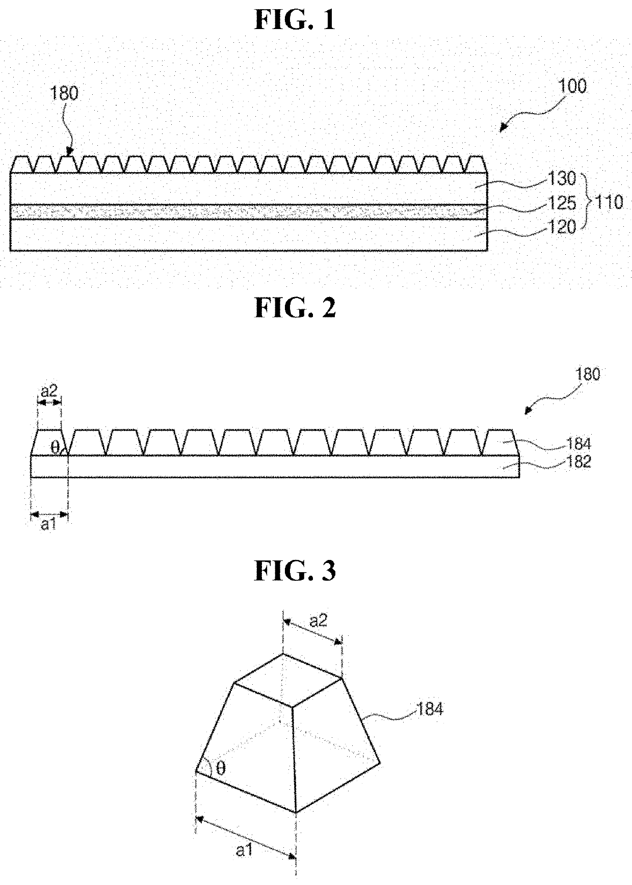
[0038]FIG. 1 is a view illustrating a display device 100 according to the present invention. Further, all the components of each display device and each microlens array according to all embodiments of the present invention are operatively coupled and configured.
[0039]Referring to FIG. 1, the display device 100 can include a display panel 110 and a microlens array 180 which is located on a front surface of the display panel 110, i.e., a surface of the display panel 110 which a picture, image or other content is displayed on.
[0040]The display panel 110 can be, but not limited to, a liquid crystal panel, an organic light emitting display panel, an electrophoresis display panel, a mini LED (light emitting diode) display panel or a micro LED display panel. However, the display panel 110 can be one of various other display panels currently known.
[0041]Further, the display panel 110 can be a tiled type display panel which is formed with a plurality of panels arranged in a tiling manner.
[00...
second embodiment
[0119]FIG. 8 is a view schematically illustrating a structure of a display device 300 according to the present invention.
[0120]Referring to FIG. 8, the display device 300 according to the second embodiment of the present invention can include a display panel 310 and a microlens array 380 located on the display panel 310.
[0121]The display panel 310 can be, but not limited to, a liquid crystal panel, an organic light emitting display panel, an electrophoresis display device, a mini LED display panel or a micro LED display panel. However, the display panel 110 can be one of various other display panels currently known. Further, the display panel 310 can be a tiled type display panel which is formed with a plurality of panels arranged in a tiling manner.
[0122]The display panel 310 can include a first substrate 320 and a second substrate 330 and a display element 325 between the first substrate 320 and the second substrate 330. In case that the display panel 310 is an organic light emitt...
PUM
| Property | Measurement | Unit |
|---|---|---|
| slanted angle θ2 | aaaaa | aaaaa |
| slanted angle θ2 | aaaaa | aaaaa |
| slanted angle θ2 | aaaaa | aaaaa |
Abstract
Description
Claims
Application Information