Display device using a semiconductor light emitting device and manufacturing method thereof

Pending Publication Date: 2022-06-16
LG ELECTRONICS INC
View PDF0 Cites 0 Cited by
  • Summary
  • Abstract
  • Description
  • Claims
  • Application Information

AI Technical Summary

Benefits of technology

The present invention is a display device that prevents contact failure between the semiconductor light emitting device and the wiring electrode. This is achieved by minimizing the flow of the anisotropic conductive layer when the semiconductor light emitting device is pressed onto the wiring substrate. Additionally, the buffer unit maintains a constant distance between the semiconductor light emitting device and the wiring electrode, ensuring even pressure application to each semiconductor light emitting device, regardless of any widening of the wiring substrate.

Problems solved by technology

The use of an anisotropic conductive layer has the advantage of being able to electrically connect the semiconductor light emitting device and the wiring electrode only by thermal compression, but there is a problem in that contact failure between the semiconductor light emitting device and the wiring electrode occurs when the area of the wiring substrate is increased.

Method used


Image

  • Display device using a semiconductor light emitting device and manufacturing method thereof
  • Display device using a semiconductor light emitting device and manufacturing method thereof
  • Display device using a semiconductor light emitting device and manufacturing method thereof

Examples


Embodiment Construction

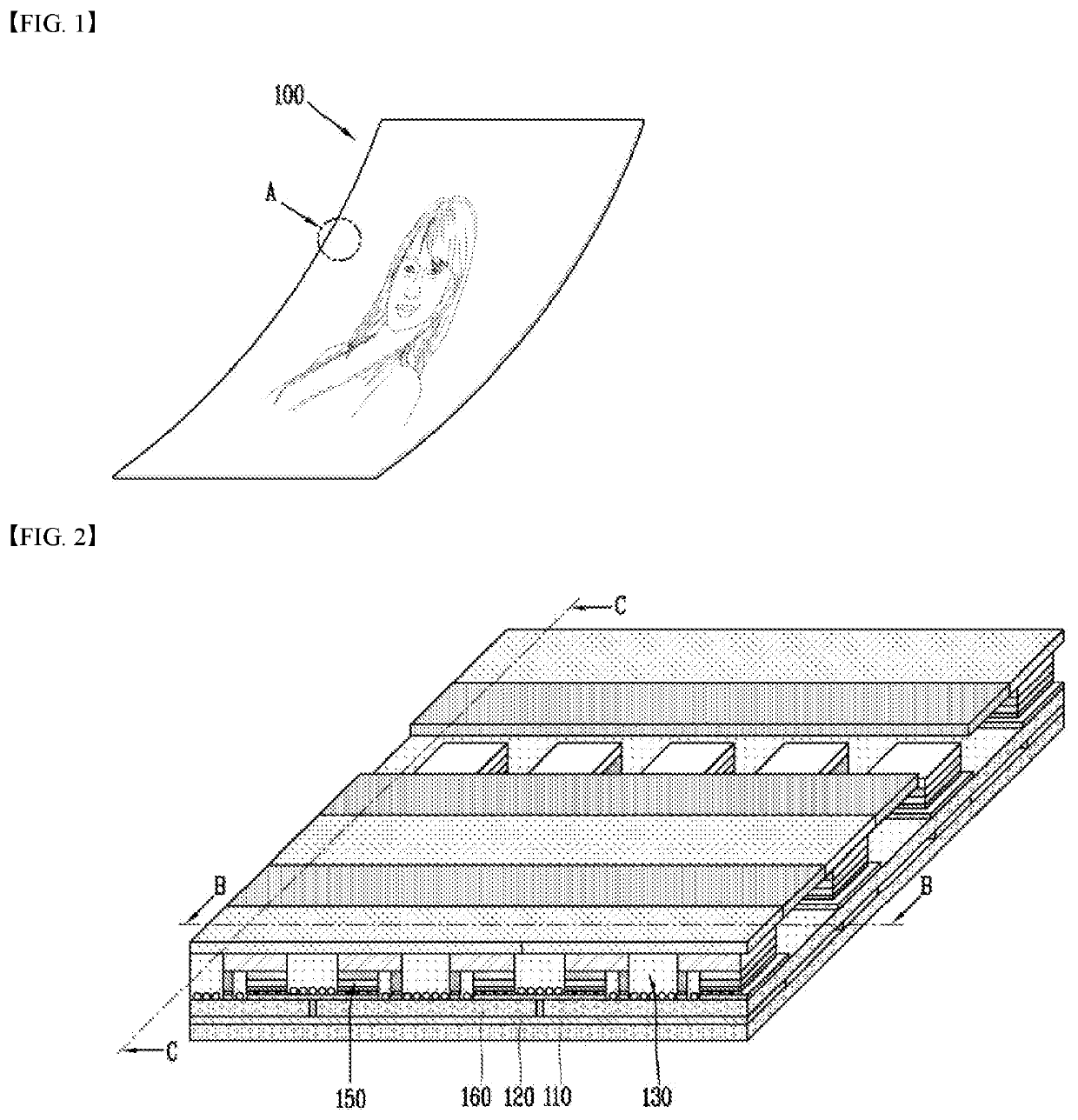
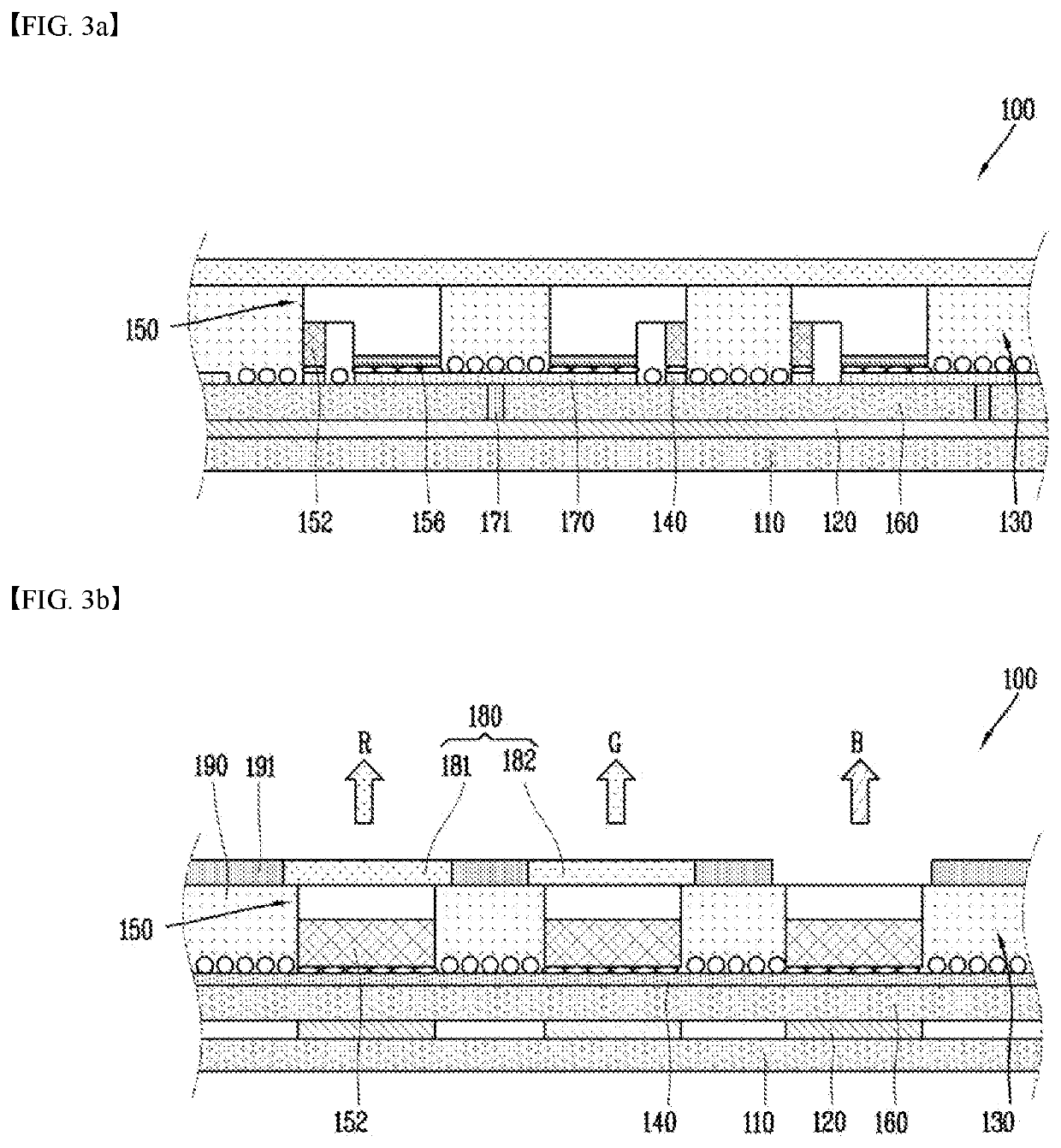
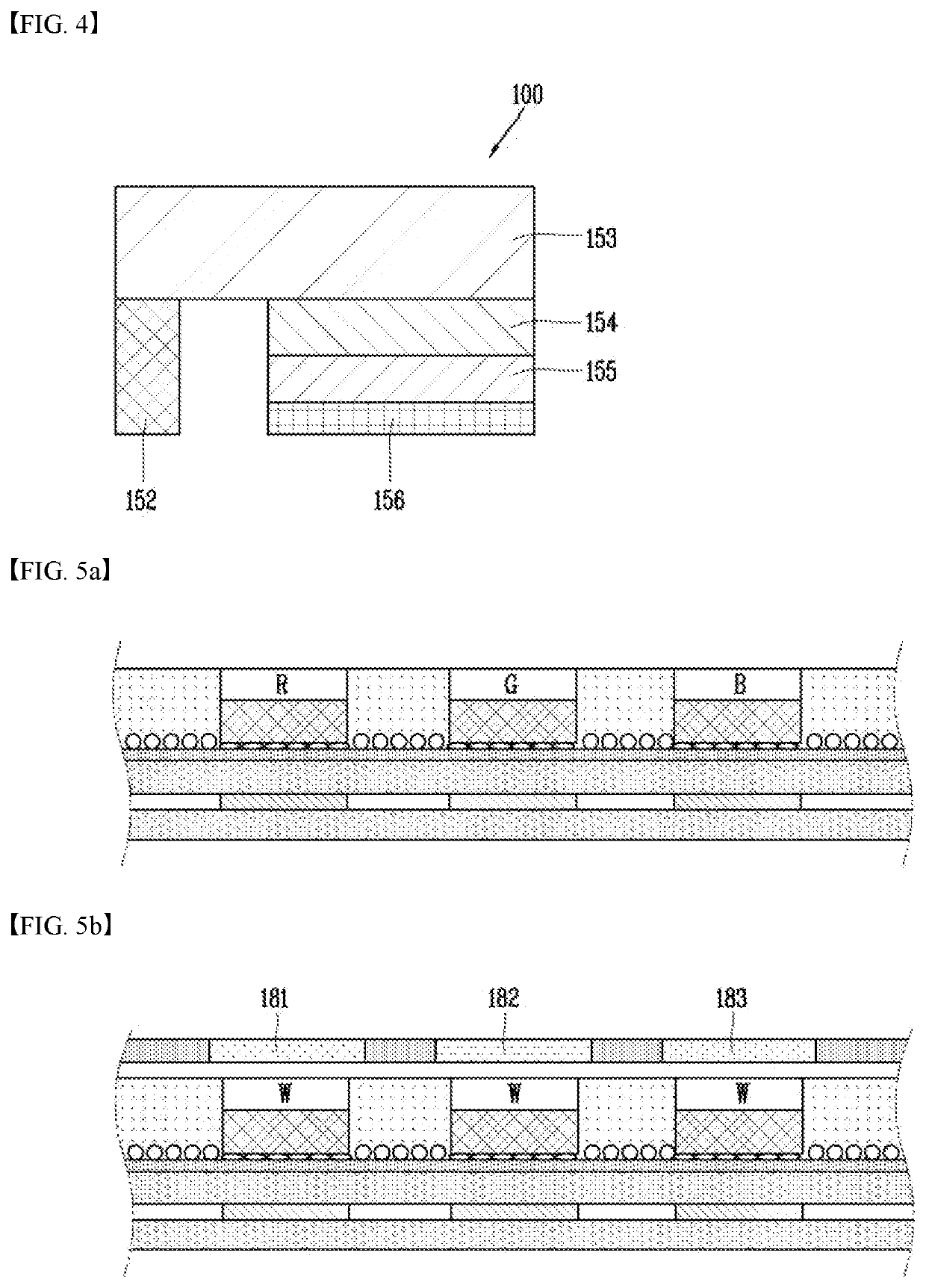
[0027]Hereinafter, exemplary embodiments disclosed in the present specification will be described in detail with reference to the accompanying drawings, but identical or similar elements are denoted by the same reference numerals regardless of reference numerals, and redundant descriptions thereof will be omitted. The suffixes “module” and “unit” for components used in the following description are given or used interchangeably in consideration of only the ease of preparation of the specification, and do not themselves have a distinct meaning or role. In addition, in describing the embodiments disclosed in the present specification, when it is determined that a detailed description of related known technologies may obscure the gist of the embodiments disclosed in the present specification, the detailed description thereof will be omitted. In addition, it should be noted that the accompanying drawings are for easy understanding of the embodiments disclosed in the present specificatio...


PUM


Abstract

The present invention includes a substrate, a wiring electrode disposed on the substrate, a plurality of semiconductor light emitting devices electrically connected to the wiring electrode, and an anisotropic conduction comprising a mixture of conductive particles and an insulating material disposed between the semiconductor light emitting devices and a light transmitting layer formed between the semiconductor light emitting devices. The anisotropic conductive layer is also formed between the wiring electrodes, and the light transmitting layer is formed on the anisotropic conductive layer formed between the wiring electrodes.

Description

TECHNICAL FIELD[0001]The present invention relates to a display device and a method of manufacturing the same, and more particularly, to a flexible display device using a semiconductor light emitting device.BACKGROUND ART[0002]In recent years, in the field of display technology, a display device having excellent characteristics such as thin and flexible has been developed. On the other hand, the main commercial displays are represented by LCD (Liquid Crystal Display) and AMOLED (Active Matrix Organic Light Emitting Diodes).[0003]Meanwhile, a light emitting diode (LED) is a well-known semiconductor light emitting device that converts current into light. As for LED, red LEDs using GaAsP compound semiconductors began to be commercialized in 1962. Since then, it has been used as a light source for display images in electronic devices including information communication devices along with GaP:N series green LEDs. Accordingly, a method of solving the above problem by implementing a flexib...

Claims


Application Information

Patent Timeline
IPC IPC(8): H01L33/62H01L33/38
CPCH01L33/62G06F1/1652H01L33/38H01L25/0753H01L33/54H01L2933/005H01L2933/0066H01L33/0093H01L2224/16225H01L27/156H01L24/14
Inventor KANG, EUNJEONGRHEE, BYUNGJOON
Owner LG ELECTRONICS INC
Why Eureka
Try Eureka