

Thin film type solar cell and method for manufacturing the same
A technology of solar cells and manufacturing methods, applied in the field of solar cells, can solve problems such as complex processes and reduced yields, and achieve the effects of reducing dead zones, increasing yields, and improving efficiency
- Summary
- Abstract
- Description
- Claims
- Application Information
AI Technical Summary
Problems solved by technology
Method used
Image

Examples
Embodiment Construction
[0040] Hereinafter, preferred embodiments of the present invention will be described in detail, examples of which are illustrated in the accompanying drawings. Wherever possible, the same reference numbers will be used throughout the drawings to refer to the same or like parts.
[0041] Hereinafter, a thin film type solar cell and a method of manufacturing the same according to the present invention will be described with reference to the accompanying drawings.
[0042]
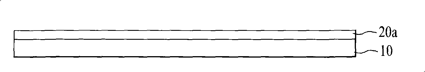
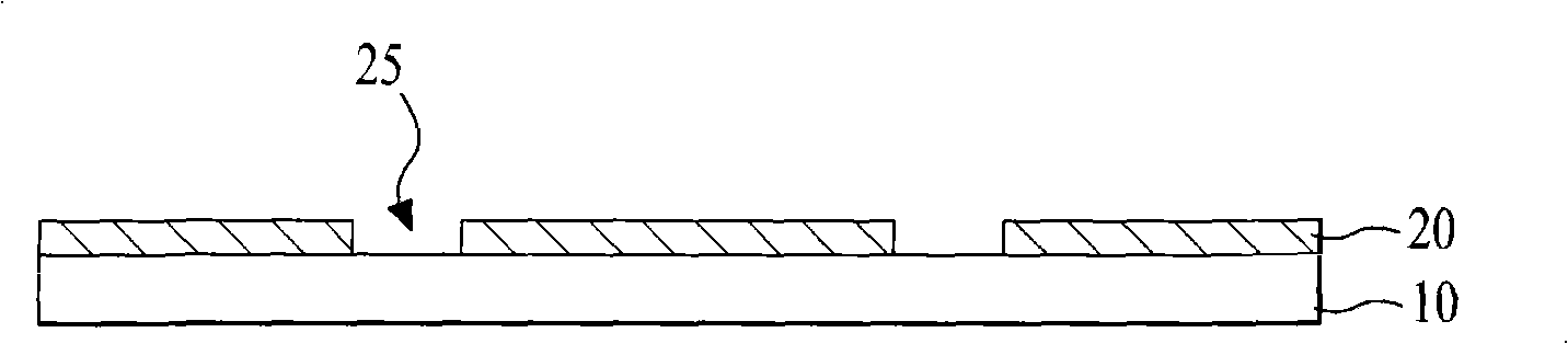
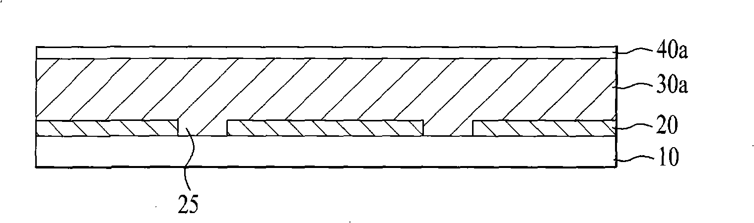
[0043] Figures 2A to 2F is a cross-sectional view showing a method of manufacturing a thin-film solar cell according to a first embodiment of the present invention.
[0044] First, if Figure 2A As shown, the front electrode layer 200a is formed on the substrate 100 .
[0045]The substrate 100 may be formed of glass or transparent plastic. The front electrode layer 200a can be made of a transparent conductive material, for example: ZnO (zinc oxide), ZnO:B (boron-doped zinc oxide), ZnO:Al (aluminum-dope...
PUM
 Abstract
Description
Claims
Application Information