

Display panel
a technology of display panel and crystal grain, which is applied in the field of display panel, can solve the problems of increasing the difficulty of crystal grain transfer, reducing the size and gap of the pads configured to be bonded to the micro light-emitting diodes, and increasing the number of crystal grain transfers of a single panel
- Summary
- Abstract
- Description
- Claims
- Application Information
AI Technical Summary
Benefits of technology
Problems solved by technology
Method used
Image

Examples
first embodiment
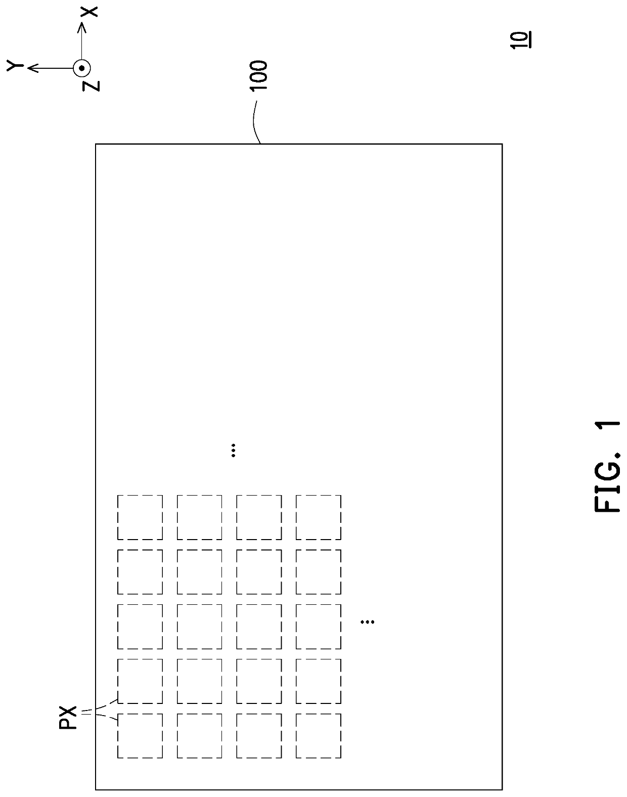
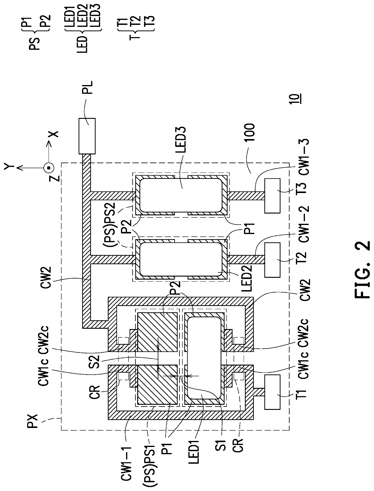
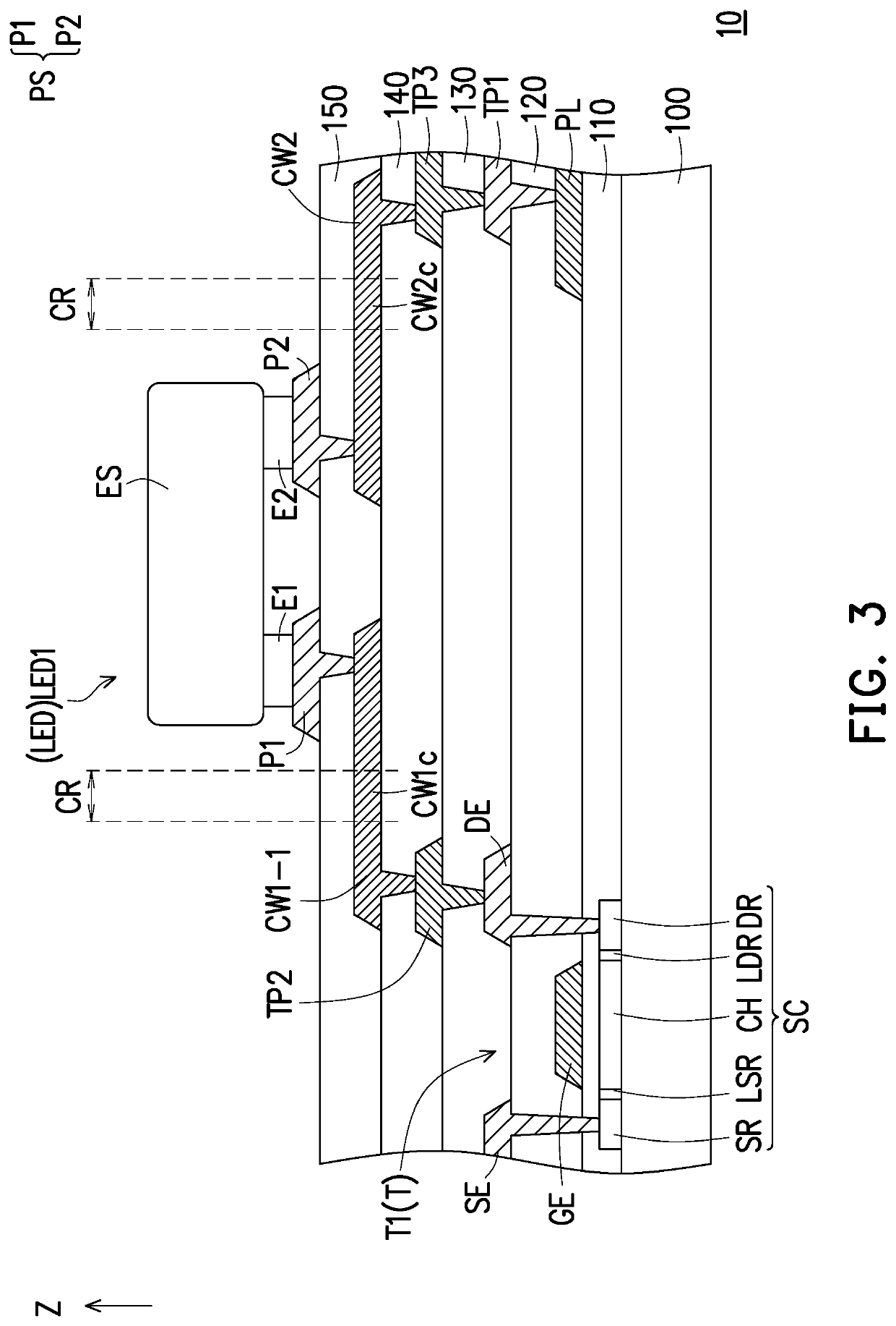
[0034]FIG. 1 is a schematic top view of a display panel according to the disclosure. FIG. 2 is a schematic diagram of a display pixel of FIG. 1. FIG. 3 is a cross-sectional schematic view of the display panel of FIG. 1. FIG. 4 is a schematic top view of the display pixel of FIG. 2 after being repaired.
[0035]With reference to FIG. 1 to FIG. 3, a display panel 10 includes a substrate 100 and a plurality of display pixels PX. The display pixels PX are disposed on the substrate 100. In this embodiment, the display pixels PX are arranged in an array. For instance, the display pixels PX are arranged in a plurality of rows and a plurality of columns in a direction X and a direction Y, but are not limited thereto. On the other hand, the display panel 10 may further include a plurality of signal lines electrically connected to the display pixels PX, such as a plurality of data lines (not shown), a plurality of scan lines (not shown), and a plurality of power lines PL. At least one data line,...
third embodiment
[0050]FIG. 5 is a schematic top view of a display panel according to the disclosure. With reference to FIG. 5, the difference between a display panel 10A of this embodiment and the display panel 10 of FIG. 2 lies in that: different numbers of pad sets configured to be bonded to the light-emitting device LED2 and the light-emitting device LED3 in the display pixel are provided. In this embodiment, in a display pixel PX-A, the numbers of pad sets PS configured to be bonded to the light-emitting device LED1, the light-emitting device LED2, and the light-emitting device LED3 are all two. Further, arrangement of two pad sets PS2A configured to be bonded to the light-emitting device LED2 and two pad sets PS3A configured to be bonded to the light-emitting device LED3 is similar to the arrangement of the two pad sets PS1 configured to be bonded to the light-emitting device LED1. Therefore, the related paragraphs of the foregoing embodiments may be referenced, and detailed description is thu...
fourth embodiment
[0055]FIG. 7 is a schematic top view of a display panel according to the disclosure. With reference to FIG. 7, the difference between a display panel 20 of this embodiment and the display panel 10 of FIG. 2 lies in that: the number of pad sets PS1 configured to be bonded to the light-emitting device LED1 in a display pixel PX-C of the display panel 20 is three. That is, the display pixel PX-C of the display panel 20 of this embodiment may repair the light-emitting device LED1 twice.
[0056]In this embodiment, the display pixel PX-C includes two cutting regions CRa and two cutting regions CRb. Among the three pad sets PS1, each of the two pad sets PS1 located outside is provided with one cutting region CRa on one side perpendicular to the arrangement direction of the first pad P1 and the second pad P2 thereof, and the two opposite sides of the pad set PS1 located between these two pad sets PS1 are provided with these cutting regions CRb in the arrangement direction of the first pad P1 ...
PUM
 Abstract
Description
Claims
Application Information