Display device and method for manufacturing display device

a display device and display technology, applied in static indicating devices, organic semiconductor devices, instruments, etc., can solve the problems of weak moisture resistance of elements, decreased light extraction efficiency, and inability to manufacture display devices of top emission or dual emission types, so as to prevent the deterioration of light-emitting elements and manufacturing display devices with much ease, the effect of high reliability

Inactive Publication Date: 2009-02-24
SEMICON ENERGY LAB CO LTD
View PDF68 Cites 50 Cited by
  • Summary
  • Abstract
  • Description
  • Claims
  • Application Information

AI Technical Summary

Benefits of technology

[0008]An object of the present invention is to provide a highly reliable display device capable of preventing the deterioration of a light-emitting element and a manufacturing method capable of manufacturing the display device with much ease.
[0021]Since a display device provided with a desiccant made of a layer containing a hygroscopic substance can be widely provided without decreasing light extraction efficiency according to the invention, the deterioration of a light-emitting element can be prevented due to an adequate hygroscopic effect of the desiccant. In addition, a complicated manufacturing step is not necessary, either. Thus, a highly reliable display device capable of displaying images with high definition and high quality can be manufactured with a favorable yield.

Problems solved by technology

An EL material (particularly an organic EL material) constituting the principal part of an EL element has properties weak in moisture and tends to be deteriorated.
These methods have a problem such as dust or contamination of heavy metal in the manufacturing steps; therefore, it is required to tackle the problem by employing a cleaning method thereof or the like.
In addition, since the depression is like ground glass and or has depression and projection with the use of mechanical processing or the like, the light extraction efficiency is decreased.
Therefore, it is inappropriate for a top emission or dual emission type display device.
In the conventional methods, a processing step of forming a depression in a sealing substrate in such a manner is necessary and apparatus necessary for the step increases, and thus the step becomes complicated.
There is possibility that a sealing substrate is damaged due to the processing step.
Therefore, there is fear that light-transmitting properties of the sealing substrate is deteriorated by being roughed and by impairing the planarity or that a thin sealing substrate is damaged.
In addition, it is difficult to form a depression in an element substrate as formed in the sealing substrate, and there is limitation on the place to provide a desiccant.

Method used


Image

  • Display device and method for manufacturing display device
  • Display device and method for manufacturing display device
  • Display device and method for manufacturing display device

Examples


embodiment mode 1

[0055]Embodiment Mode of the present invention will be described in detail with reference to the accompanying drawings. However, it is to be understood that the invention is not limited to the description below and various changes and modifications will be apparent to those skilled in the art, unless such changes and modifications depart from the content and scope of the invention. Therefore, the invention is not interpreted with limiting to the description in this embodiment mode. Note that the same reference numerals denote the same parts or parts having the same function in different drawings and the explanation will not be repeated in a constitution of the invention hereinafter explained.

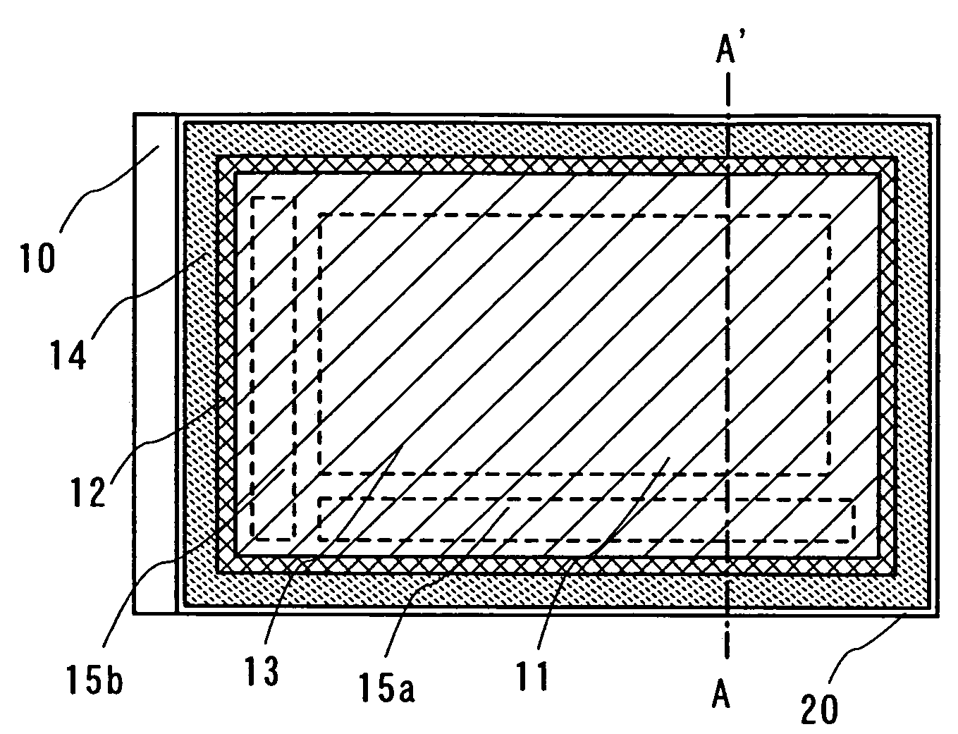
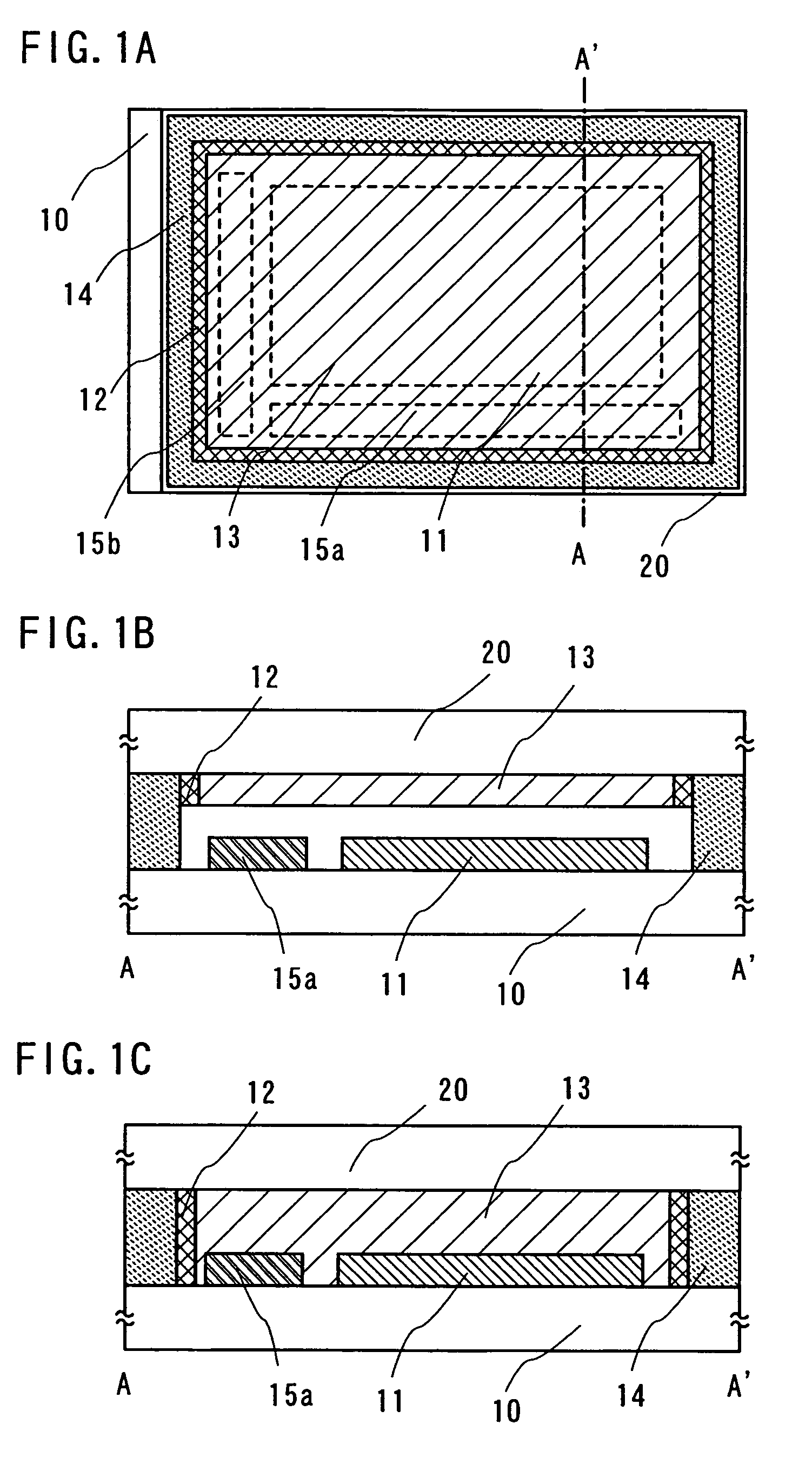
[0056]FIG. 16 is a top view showing a structure of a display panel according to the invention, where a pixel portion 2701 in which pixels 2702 are arranged in a matrix, a scanning line input terminal 2703, and a signal line input terminal 2704 are formed over a substrate 2700 having an insulatin...

embodiment mode 2

[0077]A method for manufacturing a display device of the present invention is explained in detail with reference to FIGS. 4A and 4B, FIGS. 5A and 5B, FIGS. 6A and 6B, and FIGS. 7A to 7C.

[0078]A silicon nitride oxide film (SiNO) 101a is formed to have film thicknesses of from 10 nm to 200 nm (preferably, from 50 nm to 100 nm) and a silicon oxynitride film (SiON) 101b is laminated to have film thicknesses of from 50 nm to 200 nm (preferably, from 100 nm to 150 nm) as a base film 101 over a substrate 100 having an insulating surface by a plasma CVD method. A substrate such as a glass substrate, a quartz substrate or a silicon substrate, or a metal substrate or a stainless steel substrate, in which an insulating film is formed on a surface thereof, may be used for the substrate 100. Alternatively, a plastic substrate having a heat resistance that can withstand processing temperature of this embodiment mode may be used, or a flexible substrate like a film may be also used. In addition, a...

embodiment mode 3

[0161]Examples of a top emission type and a bottom emission type that are one-sided emission types in a display device manufactured in Embodiment Mode 2 are explained in this embodiment mode with reference to FIG. 9 and FIG. 10.

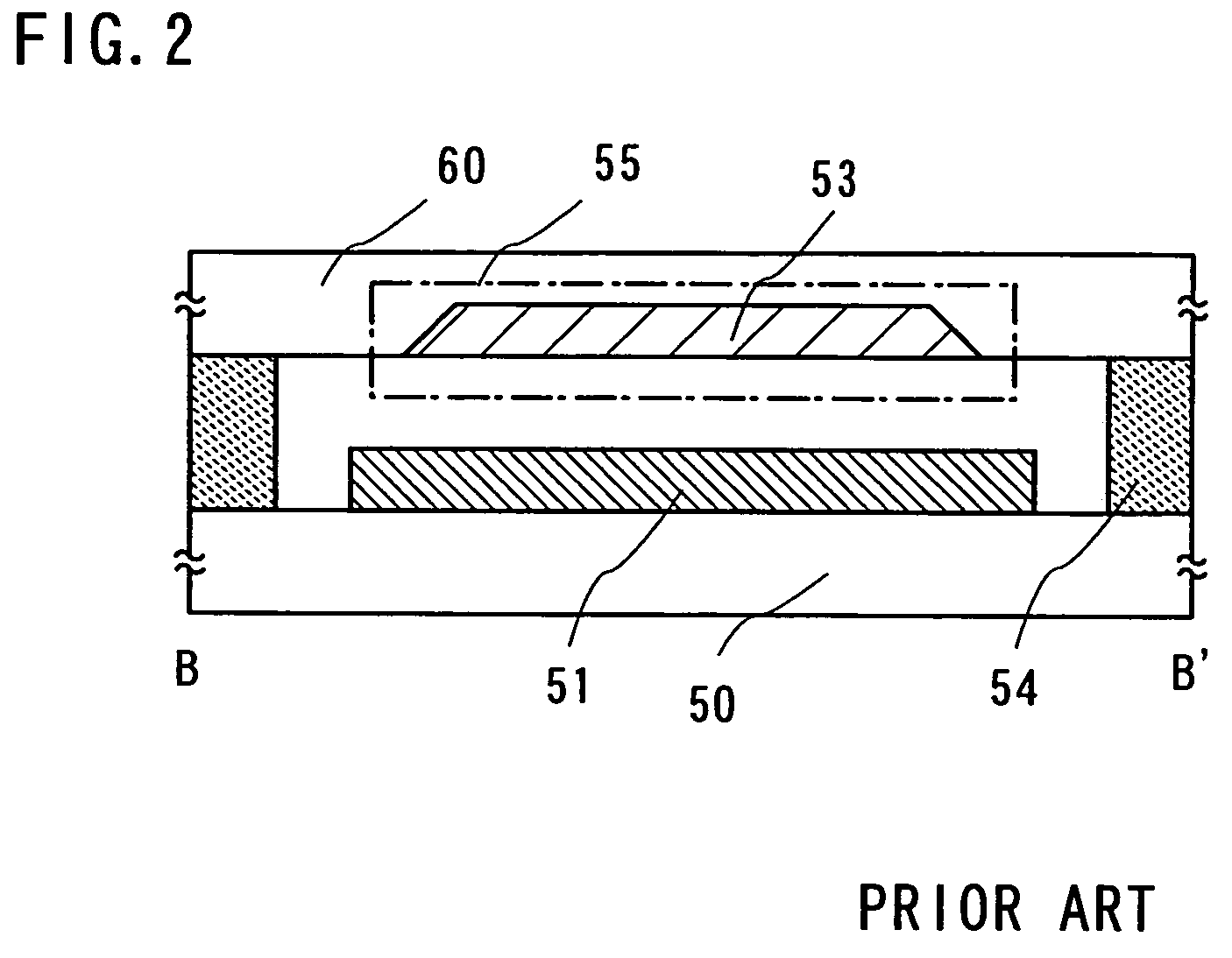
[0162]In FIG. 10, reference numeral 1700 denotes an element substrate; 1701, 1702, and 1703, TFTs; 1704, a first electrode; 1705, a light-emitting layer; 1706, a second electrode; 1707, a protective film; 1708, a filler; 1730, a frame; 1731, a layer containing a hygroscopic substance; 1709, a sealant; 1710, an insulating layer; 1711, a bank; 1712, a sealing substrate; 1720, an insulating film; 1745, a wiring layer; 1740 and 1741, terminal electrodes; 1742, an anisotropic conductive layer; and 1743, an FPC.

[0163]A display device of FIG. 10 is a bottom emission type and has a structure in which light is emitted on an element substrate side 1700 in a direction of an arrow. Note that the first electrode 1704 is formed by forming a transparent conductive film and ...


PUM


Abstract

An object of the present invention is to provide a highly reliable display device and a method for manufacturing the display device with a much easy way. According to one aspect of a method for manufacturing a display device of the invention, it comprises the steps of forming a light-emitting element over a first substrate; forming a frame to surround the light-emitting element; dropping a composition containing a liquid hygroscopic substance in a region surrounded with the frame; and forming a layer containing a hygroscopic substance by solidifying the composition, wherein the first substrate and a second substrate are adhered to each other with a sealant so that the light-emitting element, the layer containing a hygroscopic substance, and the frame are sealed between the pair of substrates.

Description

BACKGROUND OF THE INVENTION[0001]1. Field of the Invention[0002]The present invention relates to a display device having an element which sandwiches a light-emitting material between electrodes (hereinafter, a light-emitting element) and a method for manufacturing the same. Specifically, the invention relates to a display device using a light-emitting material from which EL (Electro Luminescence) can be obtained (hereinafter, an EL material).[0003]2. Description of the Related Art[0004]An EL material (particularly an organic EL material) constituting the principal part of an EL element has properties weak in moisture and tends to be deteriorated. Thus, a structure in which a desiccant is put in an EL display device (electroluminescence device) to seal is known (for example, Reference 1: Japanese Patent Laid-Open No. 2003-297558).[0005]FIG. 2 is a conventional display device, and reference numeral 50 denotes an element substrate; 51, an element portion such as a driver circuit portio...

Claims


Application Information

Patent Timeline
Patent Type & Authority Patents(United States)
IPC IPC(8): G09G3/36H01L27/32H01L31/00H01L51/00H01L51/52H05B33/02H05B33/04H05B33/10H05B33/22
CPCH01L51/5259H01L27/3244H01L27/3276H01L51/0005H01L51/529H01L2251/5315H01L2251/5323H10K71/135H10K59/12H10K59/131H10K50/846H10K50/87H10K2102/3031H10K2102/3026
Inventor HIRAKATA, YOSHIHARU
Owner SEMICON ENERGY LAB CO LTD
Why Eureka
Try Eureka